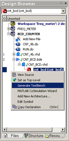
• In the Design Browser, select cnt_bcd(cnt_bcd) entity/architecture pair and invoke the pop-up menu (right click the E/A pair). Choose the Generate TestBench option
• On the first screen of the wizard, leave the default settings and click on the Next button.
5.5 Using the Testbench Wizard
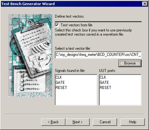
• On the second screen of the wizard, check Test vectors from file box and Browse for CNT_BCD.AWF waveform file.
• Click through the following two Next buttons and finally on the Finish button (you are accepting all the defaults for now)
5.6 Using the Testbench Wizard
• The following files are created in the TestBench folder:
– cnt_bcd_TB.vhd - test bench file for tested CNT_BCD unit,
– cnt_bcd_TB_runtest.do - the macro file for automatic compilation, simulation initialization, waveform creation and simulation
• Right Click cnt_bcd_TB_runtest.DO file and invoke the pop-up menu. Choose the Execute option. Observe signals placed on the new waveform
• Select Simulation | End Simulation from the menu
• This way, the entire simulation process was automated and fully contained in the VHDL source
6.1 Creating the top level Block Diagram
In this section we will implement the top level Block Diagram file to create our frequency meter. We will also create an FSM module Control using the top-down design method.
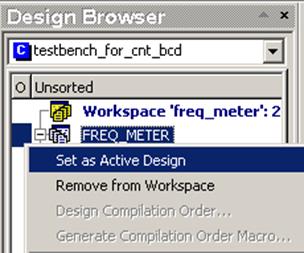
• First, call context menu for the FREQ_METER design and choose Set as Active Design
• To create the new block diagram, double click on Add New File in the Files tab in the Design Browser
• Select Wizards tab and double click on the Block Diagram Wizard
• Click Next > button
• Select VHDL in the New Source File Wizard - Language window
• Click Next > button to accept the selection
• Type top_frqm in the first edit-box in the New Source File Wizard - Name window
• Click Next >
6.2 Creating the top level Block Diagram
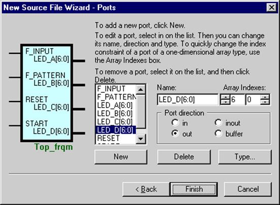
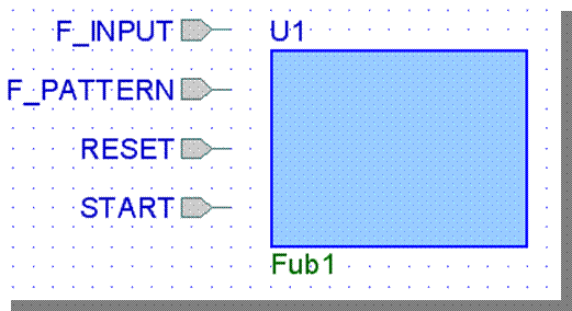
• Define the following ports of the top_frqm block diagram:
Input Ports:
- F_INPUT
- F_PATTERN
- RESET
- START
Output Ports:
- LED_A[6:0]
- LED_B[6:0]
- LED_C[6:0]
- LED_D[6:0]
• Click Finish
The Block Diagram Editor (BDE) screen with an empty diagram will
appear.
6.3 Creating the top level Block Diagram
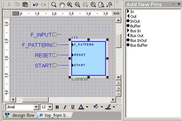
• Click the Fub button ![]() on the BDE toolbar and create a fub to the
right of the F_PATTERN, RESET and START input ports symbols by clicking in the
one corner of the fub and dragging to the opposite corner.
on the BDE toolbar and create a fub to the
right of the F_PATTERN, RESET and START input ports symbols by clicking in the
one corner of the fub and dragging to the opposite corner.
The fub you are drawing
should look like this:
NOTE: FUB is a symbol ‘in the process of creation’ and can be converted to a regular symbol when completed. The main difference between a fub and a symbol is that you can have multiple instances of the same symbol, but only one fub.
6.4 Creating the top level Block Diagram
• Click the Wire button Click the Wire button on the BDE toolbar and drag three horizontal wires from the F_PATTERN, RESET and START input port symbols to the U1 fub. Please note that three input pins are created in the fub
• on the BDE toolbar and drag three horizontal wires from the F_PATTERN, RESET and START input port symbols to the U1 fub. Please note that three input pins are created in the fub
• Hit the Esc key to return to Select mode
• Double-click the “Fub1” label below the fub
and change fub name
to CONTROL
• Right click in the fub body and select Edit to switch to the Edit mode
6.5 Creating the top level Block Diagram
• Drag Out pin from the Add New Pin
window to the fub and drop it on the right-hand edge
to create Pin1; repeat
dragging to create Pin2
• Double-click Pin1 and change
its name to GATE
Уважаемый посетитель!
Чтобы распечатать файл, скачайте его (в формате Word).
Ссылка на скачивание - внизу страницы.