B ADSP-2192 DSP PERIPHERAL REG ISTERS
Figure B-0.
Table B-0.
Listing B-0.
The DSP has general-purpose and dedicated registers in each of its functional blocks. The register reference information for each functional block includes bit definitions, initialization values, and (for I/O processor registers) memory-mapped addresses. Information on each type of register is available at the following locations:
• “Core Status Registers” on page A-8
• “Computational Unit Registers” on page A-16
• “Program Sequencer Registers” on page A-19
• “Data Address Generator Registers” on page A-26
• “Peripheral Registers” on page B-2
When writing DSP programs, it is often necessary to set, clear, or test bits in the DSP’s registers. While these bit operations can be done by referring to the bit’s location within a register or (for some operations) the register’s address with a hexadecimal number, it is much easier to use symbols that correspond to the bit’s or register’s name.
For convenience and consistency, Analog Devices provides header files that define these bit and register definitions (def2192_IO.h, def2192_PCI.h, def2192_USB.h, def2192-12.h, and def219x.h). Note that the def2192-12.h file also contains the definitions from the IO, PCI, and USB header files.
Pe riphe ra l Re g iste rs
A sample of def219x.h is shown in “Register and Bit #Defines File” on page A-28, and a sample of def2192-12.h is shown in “Register and Bit #Defines File” on page B-95.
|
! |
Many registers have reserved bits. When writing to a register, programs may clear (write zero to) the register’s reserved bits only.
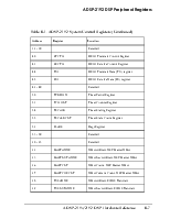
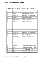
There are three groups of registers for the ADSP-2192:
• “ADSP-2192 DSP Core Registers” on page A-1
• “ADSP-2192 System Control Registers” on page B-6
• “ADSP-2192 Peripheral Device Control Registers” on page B-11
This appendix describes system control registers and peripheral device control registers. A general description of DSP peripheral architecture, which follows, provides an overview of peripheral registers.
Figure B-1 shows the DSP’s on-chip peripherals, which include the Host port (PCI or USB), AC’97 port, JTAG test and emulation port, flags, and interrupt controller.
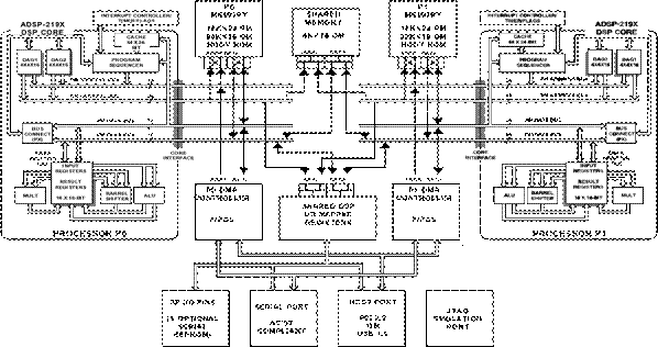
Figure B-1. ADSP-2192 Dual-Core DSP Block Diagram
The ADSP-2192 can respond to up to fourteen interrupts at any given time. A list of these interrupts can be found in the table “Interrupt Vectors for an ADSP-2192 DSP Core” on page 6-13.
The AC’97 codec port on the ADSP-2192 provides a complete synchronous, full-duplex serial interface. This interface completely supports the AC’97 standard.
The ADSP-2192 provides up to eight general-purpose I/O pins, which are programmable as either inputs or outputs. These pins are dedicated general-purpose programmable flag pins.
Pe riphe ra l De vic e Re g iste r G roup s
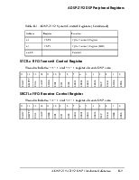
The registers that control FIFO DMA transfers are accessible only from within the DSP. They are defined as part of the Core Register Space.
Each of the DSPs integrated within the ADSP-2192 and the interfaces (PCI, USB Sub-ISA, Cardbus) needs to be capable of controlling and monitoring a variety of registers external to the DSP core. This section describes how the DSPs access these Peripheral Device Control (PDC) registers. The operation of the Peripheral Device Control (PDC) Bus that connects the DSPs and Interfaces to the PDC Registers is also described in this section.
Writes to AC’97 codec registers are posted, but only one may complete per AC’97 frame. Up to two writes may be pending at any one time. The first write completes with zero PDC wait states. A second write launched immediately after the first incurs PDC wait states equivalent to a few AC’97 BITCLKs. A third write in a row blocks for an entire AC’97 frame. Use the Frame interrupt to time AC’97 codec writes out to one per frame, assuring that they will all complete with zero wait states.
Reads from AC’97 codec registers must always wait for the data to be returned. A read must also wait for any pending AC’97 codec register writes to complete before it can begin. In the best case, a read takes one full AC’97 frame plus another three AC’97 slots (25.39 µs, or approximately 3,744 DSP cycles). This is also the typical case when the AC’97 Frame Interrupt is used to time the Read.
The worst case AC’97 read time is four frames plus three slots (87.89 µs, or approximately 12,960 DSP cycles). This occurs only when there are already two AC’97 codec register writes pending just after the start of a frame.
Most AC’97 codec registers may be shadowed, and actual reads should be rare.
Уважаемый посетитель!
Чтобы распечатать файл, скачайте его (в формате Word).
Ссылка на скачивание - внизу страницы.