11 SYSTEM DESIGN
Figure 11-0.
Table 11-0.
Listing 11-0.
This chapter describes the basic system interface
features of the ADSP-219x family processors, including the ADSP-2192. The
system interface includes various hardware and software features used to
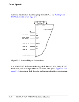
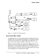
control the DSP processor. Processor control pins include a PORST![]() (power on reset) signal, clock signals, flag inputs and outputs, and interrupt
requests. This chapter describes only the logical relationships of control
signals; consult individual processor data sheets (including the data sheet for
the ADSP-2192) for actual timing specifications.
(power on reset) signal, clock signals, flag inputs and outputs, and interrupt
requests. This chapter describes only the logical relationships of control
signals; consult individual processor data sheets (including the data sheet for
the ADSP-2192) for actual timing specifications.
Some ADSP-2192 system interfaces are documented in other chapters in this book, as follows:
• “Host (PCI/USB) Port” on page 8-1 discusses the PCI, CardBus, and Sub-ISA interfaces, and includes information about how these applications use the Serial EEPROM port and the DMA (Direct Memory Access) controller. That chapter also discusses the USB interface and includes information about how USB applications use the Serial EEPROM port and the DMA controller.
• “AC’97 Codec Port” on page 9-1 discusses the AC’97 interface.
• “JTAG Test-Emulation Port” on page 10-1 discusses the JTAG Test Access Port and how it is used during emulation.
Sourc e s for A dditiona l Inform a tion
In addition, the Analog Devices web site contains a series of engineering application notes. These documents describe topics related to the ADSP-2192, including:
• Hints for porting code from ADSP-218x chips to ADSP-219x chips (described in application note EE-121)
• Tips for maximizing performance on the ADSP-219x family of processors (described in application note EE-122)
• An overview of the ADSP-219x pipeline (described in application note EE-123),
• Mechanism for booting on the ADSP-2192 (described in application note EE-124).
Engineering application notes, including any new ones that may have been added since this manual was published, are available at www.analog.com.
The ADSP-2192 processor comes in a 144-LQFP package configuration. This section provides functional descriptions of the ADSP-2192 pins.
Table 11-1 through Table 11-7 provide ADSP-2192 processor pin descriptions.
Table 11-1. PCI/USB Bus Interface Pin Descriptions
|
Pin Name(s) |
Number of Pins |
I/O |
Description |
|
AD0 - AD31 |
32 |
I/O |
Address and Data Bus |
|
CBE0 - CBE3 |
4 |
I/O |
PCI Command/Byte Enable |
|
CLK |
1 |
I |
PCI Clock |
|
CLKRUN |
1 |
O |
Clock Run |
|
DEVSEL |
1 |
I/O |
PCI Target Device Select |
|
FRAME |
1 |
I/O |
PCI Frame Select |
|
GNT |
1 |
I |
PCI Grant |
|
IDSEL |
1 |
I |
PCI Initiator Device Select |
|
INTAB |
1 |
O |
PCI / ISA Interrupt |
|
IRDY |
1 |
I/O |
PCI Initiator Ready |
|
PAR |
1 |
I/O |
PCI Bus Parity/ |
|
PCIGND |
7 |
I |
PCI Ground |
|
PCIVDD |
7 |
I |
PCI VDD supply |
|
PERR |
1 |
I/O |
PCI Parity Error/USB- (Inverting input) |
Pin De sc riptions
Table 11-1. PCI/USB Bus Interface Pin Descriptions (Continued)
|
Pin Name(s) |
Number of Pins |
I/O |
Description |
|
|
PME |
1 |
O |
PCI Power Management Event |
|
|
REQ |
1 |
O |
PCI Request |
|
|
RST |
1 |
I |
PCI Reset |
|
|
SERR |
1 |
O |
PCI System Error/USB+ (Non-inverting input) |
|
|
STOP |
1 |
I/O |
PCI Target Stop |
|
|
TRDY |
1 |
I/O |
PCI Target Ready |
Table 11-2. Crystal/Configuration Pin Descriptions
|
Pin Name(s) |
Number of Pins |
I/O |
Description |
|
BUS0 - BUS1 |
2 |
I |
PCI/ Sub-ISA/CardBus Select pins |
|
CLKSEL |
1 |
I/O |
Clock Select |
|
IGND |
1 |
I |
IGND |
|
NC |
1 |
O |
No Connect |
|
PORST |
1 |
I |
Power On Reset |
|
XTALI |
1 |
I |
Crystal Input Pin (24.576 MHz) |
|
XTALO |
1 |
O |
Crystal Output Pin |
Table 11-3. AC’97 Interface Pin Descriptions
Уважаемый посетитель!
Чтобы распечатать файл, скачайте его (в формате Word).
Ссылка на скачивание - внизу страницы.