Table 8-4. Power Management—Function Interactions (Continued)
|
Name |
Register Bits |
Comments |
|
PME Support |
Power Management Capability Bits 15:11 |
Read-only by PCI, writable by DSP. |
|
Power State |
Power Management Control/Status Bit 1:0 |
Part will be in highest power state of the three functions |
|
Reserved |
Power Management Control/Status Bit 7:2 |
Read-only, no interaction |
|
PME Enable |
Power Management Control/Status Bit 8 |
Separate for each function, no interaction |
|
Data Select |
Power Management Control/Status Bit 12:9 |
Read-only, no interaction |
|
Data Scale |
Power Management Control/Status Bit 14:13 |
Read-only, no interaction |
|
PME Status |
Power Management Control/Status Bit 15 |
Separate for each function, may be set in all functions by a wakeup |
Figure 8-1 on page 8-12 shows the relationship of the PCI clock to the ADSP-2192 internal clocks.
This domain is driven from the PCI CLK input pin, with a nominal frequency of 33 MHz. This frequency may vary from system to system. There are no controls inside the ADSP-2192 to control this clock since it is entirely under control of the Host operating system and BIOS. The PCI Clock, under control of the CLKRUN signal, may stop when the PC bus segment is powered down. This clock domain is active in PCI and CardBus modes. In Sub-ISA mode, the CLK input is not active (tied to GND). In USB mode, the PCI clock domain is inactive.
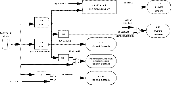
Figure 8-1. Clock Domains
Because each DSP may try to access the I/O registers simultaneously, hardware has been added to control access to the register bus and eliminate conflicts. The PCI interface and the USB interface access the same set of registers and use the same internal register access bus. (The USB interface cannot access registers in the PCI clock domain, and the PCI interface cannot access registers within the USB clock domain.)
Prioritization between the different possible masters is fixed. The priorities from highest to lowest are: DSP #1, DSP #2, Host (PCI/USB) interface.
When employed in a multiprocessing system, the ADSP-2192 must perform uninterrupted sequences of register bus accesses. Although these accesses may be required infrequently, they are essential in certain cases.
To this end, a Lock function is provided.
To Lock the Bus, the DSP writes a “1” to Bit7 of the FLAGS register. This Flag output bit is assigned to the Bus Lock Request functionality and generates a continuous request on the Peripheral Device Control Bus. Once the Bus is granted to the DSP, it remains granted until the bit is cleared. The DSP can check to see if the bus has been granted by examining Bit15 of the FLAGS register. A “1” in this bit indicates that the bus has been granted to the DSP.
Once the Bus is Locked, the DSP can perform Read-Modify-Write operations without the danger of the other DSP or the PCI/USB interface changing the register. Avoid locking the Bus for extended periods of time.
The PDC bus is a shared resource that affects almost all aspects of operation of an ADSP-2192 system. Transactions may be initiated by either DSP or by the external bus interface (whether PCI, USB or sub-ISA).
Transactions may be targeted at registers for PCI, USB, system control, AC’97, and GPIO functions. Only one transaction may be in progress at a time; all other initiators must wait for the current transaction to complete.
Уважаемый посетитель!
Чтобы распечатать файл, скачайте его (в формате Word).
Ссылка на скачивание - внизу страницы.