a Technical Note
ONE TECHNOLOGY WAY•P.O.BOX 9106• NORWOOD, MASSACHUSETTS 02062-9106 •781/329-4700
800 to 2500 MHz Single-Sideband Upconversion of Quadrature DDS Signals
by: Richard Cushing, NI7X
DDS (direct digital synthesis) technology is rapidly advancing; however, direct synthesis of UHF and microwave output frequencies is not presently practical or economically feasible. Usually, DDSs are integrated with a high-frequency PLL or upconverted in a mixer to take advantage of the DDS’ attributes at UHF and above.
This paper will offer an economical approach to frequency up-conversion using the AD8346 Quadrature Modulator and the AD9854 Quadrature DDS. The resulting suppressed-carrier, single-sideband signal displays LO (local oscillator) and undesired sideband rejection of >36dB. 36dB of unwanted signal rejection may not be adequate for some applications, but this >3000x reduction of unwanted sideband power will greatly reduce output filter complexity or make an impossible filtering task “do-able”. Switching from “upper” to “lower” sideband is simply a matter of reversing the DDS signal connections to the AD8346 modulator.
The AM, FM and FSK modulation capabilities of the AD9854 DDS enhance the utility of this application by providing digital and analog communications capability.
PLL multiplication of a DDS signal to UHF and above is easily accomplished but there are significant consequences which diminish practically every DDS attribute. Degradation will occur in phase noise specification, new frequency acquisition time, loss of frequency resolution and spurious-free dynamic range (SFDR).
DDS output phase noise will degrade
 |
|||
 |
|||
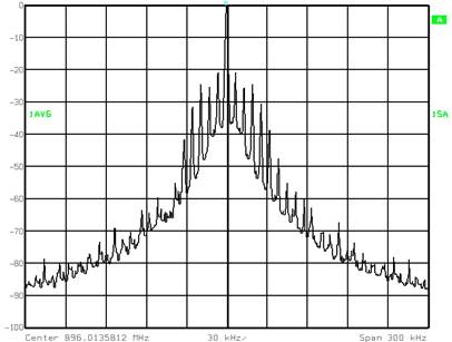
Figure 2: PLL output signal at 896 MHz (multiplied by 64x). PLL loop bandwidth is readilyobserved by examining the change in spur levels signals within the PLL loop bandwidth. Phase noise degradation is very apparent.
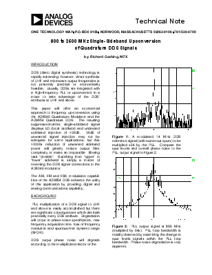
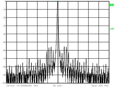
PLL: 20LOG(Fout/Fin). For example, if a DDS signal at 10 MHz is multiplied by 100 to yield an output of 1 GHz from a PLL, output phase noise within the PLL loop bandwidth will degrade by 40dB relative to the DDS input signal phase noise. Furthermore, spurious signals will be augmented by the same amount. An acceptable –60 dB spur at the PLL input may be amplified to an unacceptable –20 dB level at the PLL output.
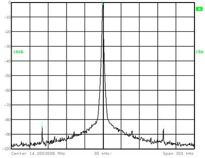
Figure 2 illustrates the effect of PLL loop bandwidth on spur amplification and phase noise degradation. Compare to the phase noise skirt and spur levels of the DDS input signal in Figure 1. Spurs located above the PLL loop bandwidth cutoff frequency (approximately 30 kHz in the example) do not experience the same amplification as those within the bandwidth.
The integration of a PLL with a DDS reference input negates one of the DDS’ notable attributes: agility. Frequency agility becomes a function of how rapidly the PLL can lock to frequency changes of the DDS. Frequency “lock time” can easily be increased by a factor of 10,000 (from 10 nanoseconds to 100 microseconds).
Finally, the extremely fine frequency resolution of the DDS will also be affected when integrated with a xN PLL. For example, if the DDS output is incremented by 1 Hz, a x64 PLL will increment its output by 64 Hz. Similarly, any phase or frequency instability of the DDS reference clock will be multiplied by N in the PLL. Phase noise and timing “jitter” are examples of “phase instability”.
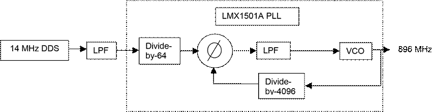
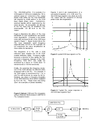
Figure 5 (below): DDS and PLL integration using a National Semiconductor
LMX1501A PLL evaluation board.
 |
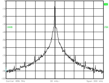 |
Figure 4: Typical PLL output response to the DDS input signal at Fig.3 .
Уважаемый посетитель!
Чтобы распечатать файл, скачайте его (в формате Word).
Ссылка на скачивание - внизу страницы.