Digital Transmitter of Phase Modulated Signals Based on DSP
Robert Kotrys, Piotr Remlein and Pawel Szulakiewicz
Poznan University of Technology
Institute of Electronics & Telecommunications ul. Piotrowo 3a, 60-965 Poznan, POLAND
E-mail: Robert.Kotrys@et.put.poznan.pl, Piotr.Remlein@et.put.poznan.pl, Pawel.Szulakiewicz@et.put.poznan.pl
|
ABSTRACT In this paper, we describe an implementation of such digital transmitter consisting of digital signal processor (ADSP 2111) and controlled by it numeric control oscillator (NCO) AD 7008. Data modulated signal is generated on intermediate frequency (IF) 1. INTRODUCTION In the last years many interesting digital modulation techniques were presented in the |
good properties, they are bandwidth and power efficient and noise resistant. There is need for precise and flexible digital transmitters that offer such features as programmability, temperature insensivity, reduced cost, easiness to design etc. [].We describe an implementation of such digital transmitter consisting of digital signal processor (DSP) (ADSP 2111) and controlled by it NCO (AD7008). The AD7008 chip is able to generate sinusoidal carrier up to 25 MHz and is able to provide phase modulation, frequency modulation, and amplitude modulation in both in-phase and quadrature channels. It provide great programmability software depend modulation. An example of DSP assembler language program of trellis modulation scheme will be included. |
literature [...]. The new modulation schemes have
Fig A. Block diagram of AD7008 chip
2. AD7008 DESCRIPTION
In contrast to previous digital synthesiser devices, the AD7008 an exciting new level of integration for the RF/Communications system designer.
The AD7008 direct digital
|
|
memory. The ADSP2111 has 1K words of data memory and 2K words of program memory RAM on chip. Standard Analog Devices ADSP evaluation board is used in laboratory model of the transmitter. Simply glue logic (as port decoder) was necessary to join NCO with processor board. An analog part consist of single IF amplifier with
supported. Frequency accuracy can be controlled to one part in
4 billion. Modulation may be affected by loading registers either trough the parallel microprocessor interface or serial interface.
The main component of the NCO is a 32-bit phase accumulator witch accumulates a phase step on every clock cycles. The value of phase step determines haw many clocks cycles are required for the phase accumulator for the count 2π radians. The output frequency is given by:
fOUT =∆Phse232 fCLOCK (1)
Complex frequency modulation schemes as GMSK, can be implemented by updating the contents of phase step register. Following the NCO, a phase offset can be added to perform phase modulation (as MPSK) using the 12-bit phase register. Phase is converted to amplitude signal by means of Sine/Cosine ROM Look Up Table (LUT). Two 10-bit amplitude multipliers are provided (follow LUT) allowing the easy implementation of either Quadrature Amplitude Modulation (QAM) or Amplitude Modulation (AM). However, there is no internal clipping logic to prevent overflow.
The described digital transmitter is controlling by ADSP2111. It is a fixed point, fast, low cost, single-chip microcomputer optimised for digital signal processing (DSP). It combines CPU with two serial ports, a host interface port, programmable timer, extensive interrupt capabilities, on-chip program and data RAM simple LC band pass filter. The great power of the transmitter is based on software solution.
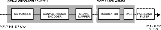
As an example, in this paper we will described a software solution of V.32 recommendation transmitter. The described transmitter consist of a scrambler, convolutional encoder, mapper and modulator. The assembler routins are in apendix.
The first three parts are software implemented on the digital signal processor. The last function signal generation and modulation is done by the NCO. This partition of the transmitter and task assignment to software and hardware makes possible to obtain suitable transmission rate, hardware efficiency and flexibility.
A data bit-stream is scrambled previous. A self-synchronising scramblers are in V.32 modem, each transmission direction uses a different scrambler. The next parts of the transmitter consist of differential encoder, convolutional encoder, mapper and modulator, solution of this parts we will present. The diagram of the transmitter is shown on figure @. Each of

Fig C. Encoder scheme.
this part are done by separate assembler function.
Уважаемый посетитель!
Чтобы распечатать файл, скачайте его (в формате Word).
Ссылка на скачивание - внизу страницы.
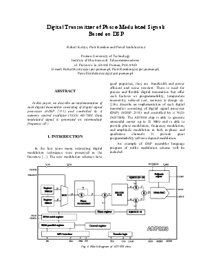
 synthesis chip is numerically controlled oscillator
employing a 32-bit phase accumulator, sine and cosine look-up tables and
10-bit D/A converter integrated on a single CMOS chip. Clock rates up to 50
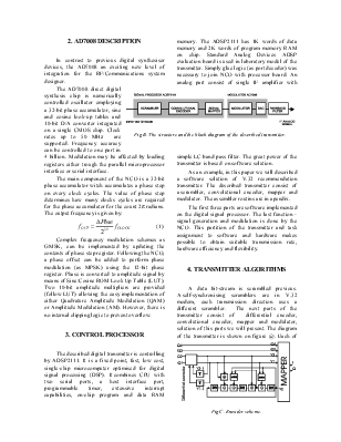
MHz are Fig B. The
structure and the block diagram of the described transmitter.
synthesis chip is numerically controlled oscillator
employing a 32-bit phase accumulator, sine and cosine look-up tables and
10-bit D/A converter integrated on a single CMOS chip. Clock rates up to 50
MHz are Fig B. The
structure and the block diagram of the described transmitter.