a Complete DDSCMOS
AD9830
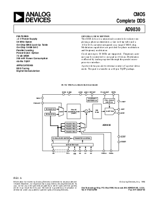
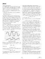
+5 V Pow er S upply This DDS device is a numerically controlled oscillator em50 MHz S peed ploying a phase accumulator, a sine look-up table and a
On-C hip S INE L ook-Up Table 10-bit D/A converter integrated on a single CMOS chip. On-C hip 10-Bit DAC Modulation capabilities are provided for phase modulation
Parallel L oading and frequency modulation.
Pow er-Dow n Option Clock rates up to 50 MHz are supported. Frequency accu72 dB S FDR racy can be controlled to one part in 4 billion. Modulation
250 m W Pow er C onsum ption is effected by loading registers through the parallel micro48-Pin TQFP processor interface.
APPL IC ATIONS A power-down pin allows external control of a power-down
DDS Tuning mode. The part is available in a 48-pin TQFP package.
Dig ital Dem odulation

REV. A
Information furnished by Analog Devices is believed to be accurate and © Analog Devices, Inc., 1996 reliable. However, no responsibility is assumed by Analog Devices for its use, nor for any infringements of patents or other rights of third parties which may result from its use. No license is granted by implication or One Technology Way, P.O. Box 9106, Norwood, MA 02062-9106, U.S.A.
otherwise under any patent or patent rights of Analog Devices. Tel: 617/329-4700 Fax: 617/326-8703
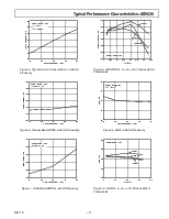
AD9830–SPECIFICATIONS1 (VDD
= +5 V 6 5%; AGND = DGND = 0 V; T![]() A = TMIN
to TMAX; REFIN = REFOUT;
A = TMIN
to TMAX; REFIN = REFOUT;
Уважаемый посетитель!
Чтобы распечатать файл, скачайте его (в формате Word).
Ссылка на скачивание - внизу страницы.