|
LM143/LM343 High Voltage Operational Amplifier General Description Features The LM143 is a general purpose high voltage operational Y Wide supply voltage range g4.0V to g40V amplifier featuring operation to g40V, complete input over- Y Large output voltage swing g37V voltage protection up to g40V and input currents compara- Y Wide input common-mode range g38V ble to those of other super-b op amps. Increased slew rate, Y Input overvoltage protection Full g40V together with higher common-mode and supply rejection, Y Supply current is virtually independent of supply voltage insure improved performance at high supply voltages. Oper- and temperature ating characteristics, in particular supply current, slew rate and gain, are virtually independent of supply voltage and Unique Characteristics temperature. Furthermore, gain is unaffected by output loading at high supply voltages due to thermal symmetry on Y Low input bias current 8.0 nA the die. The LM143 is pin compatible with general purpose Y Low input offset current 1.0 nA op amps and has offset null capability. Y High slew rateÐessentially independent of temperature Application areas include those of general purpose op and supply voltage 2.5V/ms amps, but can be extended to higher voltages and higher Y High voltage gainÐvirtually independent of resistive output power when externally boosted. For example, when loading, temperature, and supply voltage 100k min used in audio power applications, the LM143 provides a Y Internally compensated for unity gain power bandwidth that covers the entire audio spectrum. In Y Output short circuit protection addition, the LM143 can be reliably operated in environ- Y Pin compatible with general purpose op amps ments with large overvoltage spikes on the power supplies, where other internally-compensated op amps would suffer catastrophic failure. The LM343 is similar to the LM143 for applications in less severe supply voltage and temperature environments. |
|
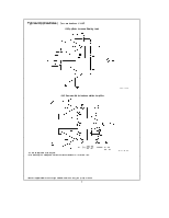
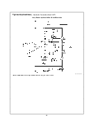
Connection Diagram Metal Can Package Top View
TL/H/7783–1 Order Number LM143H, LM143H/883* or LM343H See NS Package Number H08C *Available per SMDÝ 7800303 |
|
Absolute Maximum Ratings (Note 1) If Military/Aerospace specified devices are required, please contact the National Semiconductor Sales Office/ Distributors for availability and specifications. (Note 4) LM143 LM343 Supply Voltage g40V g34V Power Dissipation (Note 1) 680 mW 680 mW Differential Input Voltage (Note 2) 80V 68V Input Voltage (Note 2) g40V g34V Operating Temperature Range b55§C to a125§C 0§C to a70§C Storage Temperature Range b65§C to a150§C b65§C to a150§C Output Short Circuit Duration 5 seconds 5 seconds Lead Temperature (Soldering, 10 sec.) 300§C 300§C ESD rating to be determined. Electrical Characteristics (Note 3) |
||||||||
|
Parameter |
Conditions |
LM143 |
LM343 |
Units |
||||
|
Min |
Typ |
Max |
Min |
Typ |
Max |
|||
|
Input Offset Voltage |
TA e 25§C |
2.0 |
5.0 |
2.0 |
8.0 |
mV |
||
|
Input Offset Current |
TA e 25§C |
1.0 |
3.0 |
1.0 |
10 |
nA |
||
|
Input Bias Current |
TA e 25§C |
8.0 |
20 |
8.0 |
40 |
nA |
||
|
Supply Voltage Rejection Ratio |
TA e 25§C |
10 |
100 |
10 |
200 |
mV/V |
||
|
Output Voltage Swing |
TA e 25§C, RL t 5 kX |
22 |
25 |
20 |
25 |
V |
||
|
Large Signal Voltage Gain |
TA e 25§C, VOUT e g10V, RL t 100 kX |
100k |
180k |
70k |
180k |
V/V |
||
|
Common-Mode Rejection Ratio |
TA e 25§C |
80 |
90 |
70 |
90 |
dB |
||
|
Input Voltage Range |
TA e 25§C |
g24 |
g26 |
g22 |
g26 |
V |
||
|
Supply Current (Note 5) |
TA e 25§C |
2.0 |
4.0 |
2.0 |
5.0 |
mA |
||
|
Short Circuit Current |
TA e 25§C |
20 |
20 |
mA |
||||
|
Slew Rate |
TA e 25§C, AV e 1 |
2.5 |
2.5 |
V/ms |
||||
|
Power Bandwidth |
TA e25§C, VOUT e 40 Vp-p, RL e 5 kX, THD s 1% |
20k |
20k |
Hz |
||||
|
Unity Gain Frequency |
TA e 25§C |
1.0M |
1.0M |
Hz |
||||
|
Input Offset Voltage |
TA e Max TA e Min |
6.0 6.0 |
10 10 |
mV |
||||
|
Input Offset Current |
TA e Max TA e Min |
0.8 1.8 |
4.5 7.0 |
0.8 1.8 |
14 14 |
nA |
||
|
Input Bias Current |
TA e Max TA e Min |
5.0 16 |
35 35 |
5.0 16 |
55 55 |
nA |
||
|
Large Signal Voltage Gain |
RL t 100 kX, TA e Max RL t 100 kX, TA e Min |
50k 50k |
150k 220k |
50k 50k |
150k 220k |
V/V |
||
|
Output Voltage Swing |
RL t 5.0 kX, TA e Max RL t 5.0 kX, TA e Min |
22 22 |
26 25 |
20 20 |
26 25 |
V |
||
|
Note 1: Absolute maximum ratings are not necessarily concurrent, and care must be taken not to exceed the maximum junction temperature of the LM143 (150§C) or the LM343 (100§C). For operating at elevated temperatures, devices in the H08 package must be derated based on a thermal resistance of 155§C/W, junction to ambient, or 20§C/W, junction to case. Note 2: For supply voltage less than g40V for the LM143 and less than g34V for the LM343, the absolute maximum input voltage is equal to the supply voltage. Note 3: These specifications apply for VSeg28V. For LM143, TAe max e 125§C and TAe min eb55§C. For LM343, TAe max e 70§C and TAe min e 0§C. Note 4: Refer to RETS143X for LM143H and LM1536H military specifications. Note 5: The maximum supply currents are guaranteed | ||||||||
Уважаемый посетитель!
Чтобы распечатать файл, скачайте его (в формате Word).
Ссылка на скачивание - внизу страницы.