Another option available to the designer is to upconvert a DDS signal to UHF/microwave frequencies using a mixer. Upconverting does not increase either the spur levels or the phase noise. Furthermore, frequency agility and resolution remain unaffected. The largest obstacle to overcome is the presence of the double-sideband (DSB) output: LO + DDS and LO – DDS.
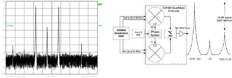
Figure 6 shows a 200 MHz region of spectrum of a standard-configuration mixer
output. In this instance, the two sidebands are 50 MHz apart. This is only 5%
of the 1 GHz output frequency. Filtering the signals to remove the unwanted
sideband will be extremely difficult. Increasing the output frequency to 2 GHz
may complicate matters to the point where filtering is impractical.
Figure 6: DSB output from typical mixer
One could incorporate multiple stages of mixing and filtering to produce a DSB signal (from a “low” frequency DDS) with larger sideband spacing at UHF/microwave that will be more easily filtered but at additional expense and complexity.
There is an alternative approach to solving the problem of suppressing the unwanted sideband. That approach is to mix the LO (local oscillator) and DDS signals - both in quadrature (90 degrees out of phase) – and then combine them such that one sideband is augmented in the summation and the other sideband is diminished. This method of sideband cancellation is not new. In fact, it has been around for about 50 years and is commonly known as the “phasing method” of single sideband generation.
The AD8346 Quadrature Modulator will provide impressive SSB performance from 800 MHz to 2.5 GHz. Specifically, the designer can upconvert a dc – 70 MHz signal to any region in the .8 to 2.5 GHz bandwidth and obtain unwanted sideband rejection of 36 dB (typical). The upconverted signal may be a single frequency or any combination of signals within the allowable input bandwidth. Figure 7 shows how the AD9854 DDS quadrature output signals can be fed to the AD8346 differential “baseband modulation” inputs for SSB upconversion near the LO frequency.
Figure 7: Quadrature SSB upconversion block diagram with the AD9854 Quadrature DDS and the AD8346 Quadrature
Modulator.
In quadrature upconversion as in Figure 7, two mixers are operated in quadrature (sine and cosine LO’s are mixed with I & Q baseband signals) and the two mixer outputs are summed internally to perform mathematical operations according to the phase relationships and signs of the frequency components. In this manner, the quadrature “modulator” augments one sideband and diminishes the other while suppressing the LO.
For a more complete explanation, including a basic mathematical analysis of analog and digital quadrature modulation and SSB upconversion the reader is directed to an article written by Doug Smith, “Signals, Samples and Stuff: A DSP Tutorial (Part 1)” in the Mar/Apr 1998 issue of QEX: Forum for Communications Experimenters magazine. For more information contact American Radio Relay League, 225 Main Street, Newington, CT 06111.
Implementation of the SSB upconverter in the lab was accomplished using two Analog Devices evaluation boards for the AD9854 and the AD8346. Modifications to the AD8346 evaluation board were required to accept the filtered, quadrature, single-ended signals provided by the AD9854 evaluation board. The output voltage levels also needed to be increased to suit the AD8346 input requirements. Modifications are as follows:
1. Add two 1:16 center-tapped impedancestep-up transformers (Mini-circuits T166T) to convert single-ended quadrature signals to differential signals and to provide a 1:4 voltage step-up. Use of the center-tapped secondary allowed a dc offset voltage of 1.2 volts to be added to the differential signals to comply with the AD8346 input requirements.
2. Add 1K termination resistors acrosseach transformer output.
3. Add a 1.2-volt dc bias source consistingof two silicon diodes forward biased from the 3.3 volt supply voltage through a 2K current limiting resistor. Connect to center-tap of both I and Q channel transformer secondary windings.
Tests of this setup verified the performance expectations conveyed in the AD8346 data sheet when the quadrature input signals from the AD9854 were properly adjusted to compensate for quadrature phase error and I & Q amplitude imbalance. See Fig 8.
Уважаемый посетитель!
Чтобы распечатать файл, скачайте его (в формате Word).
Ссылка на скачивание - внизу страницы.