|
|
C1995 National Semiconductor Corporation TL/W/11814 RRD-B30M115/Printed in U. S. A.
|
Pin Description |
|||
|
Pin No. |
Pin Name |
I/O |
Description |
|
1 |
VCC M |
I |
Voltage supply for the mixer. The input voltage level to this pin should be a DC Voltage ranging from 2.85V to 3.15V. |
|
2 |
GND |
Ground |
|
|
3 |
LNAIN |
I |
RF input signal to the LNA. External DC blocking capacitor is required. |
|
4 |
GND |
Ground |
|
|
5 |
GND |
Ground |
|
|
6 |
RFIN |
I |
RF input to the mixer. The RF signal to be down converted is connected to this pin. External DC blocking capacitor is required. |
|
7 |
GND |
Ground |
|
|
8 |
PWDN |
I |
Power down signal pin. Both the LNA and mixer are powered down when a HIGH level is applied to this pin (VIH). |
|
9 |
IFOUT |
O |
IF output signal of the mixer. External DC blocking capacitor is required. |
|
10 |
GND |
Ground |
|
|
11 |
LOIN |
I |
Local oscillator input signal to the mixer. External DC blocking capacitor is required. |
|
12 |
GND |
Ground |
|
|
13 |
GND |
Ground |
|
|
14 |
LNAOUT |
O |
Output of the LNA. This pin outputs the amplified RF signal. External DC blocking capacitor is required. |
|
15 |
GND |
Ground |
|
|
16 |
VCC A |
I |
LNA supply Voltage. DC Voltage ranging from 2.85V to 3.15V. |
|
Absolute Maximum Ratings Recommended Operating If Military/Aerospace specified devices are required, Conditions please contact the National Semiconductor Sales Office/Distributors for availability and specifications. CC) 2.85V–3.15V Supply Voltage (V Supply Voltage (VCC) 6.5V A) b10§C to a70§C Operating Temperature (T Storage Temperature (TS) b65§C to a150§C IN 0.1 GHz to 2.0 GHz RF LO Operating Temperature (TO) b40§C to a85§C IN 0.1 GHz to 2.0 GHz |
|||
|
Electrical Characteristics: LNA (VCC ea3.0V g5%, TA e 25§C, Zo e 50X and fIN e 2.0 GHz @b30 dBm unless otherwise specified.) |
|||||||||||||
|
Symbol |
Parameter |
Conditions |
Min |
Typ |
Max |
Units |
|||||||
|
ICC |
Supply Current |
In Operation |
6.5 |
8.0 |
mA |
||||||||
|
ICC-PWDN |
Supply Current |
In Power Down Mode |
10 |
mA |
|||||||||
|
G |
Gain |
9 |
10 |
dB |
|||||||||
|
P1dB |
Output 1 dB Compression Point |
b5.0 |
b3.0 |
dBm |
|||||||||
|
OIP3 |
Output 3rd Order Intercept Point |
5.0 |
7.0 |
dBm |
|||||||||
|
NF |
Single Side Band Noise Figure |
4.8 |
6.0 |
dB |
|||||||||
|
RLIN |
Input Return Loss |
10 |
15 |
dB |
|||||||||
|
RLOUT |
Output Return Loss |
10 |
11 |
dB |
|||||||||
|
Electrical Characteristics: Mixer (VCC ea3.0V g5%, TA e 25§C, Zo e 50X, fRF e 2.0 GHz @ b30 dBm, fLO e 1.89 GHz @ 0 dBm; fIF e 110 MHz unless otherwise specified.) |
|||||||||||||
|
Symbol |
Parameter |
Conditions |
Min |
Typ |
Max |
Units |
|||||||
|
ICC |
Supply Current |
In Operation |
9.0 |
12.0 |
mA |
||||||||
|
ICC-PWDN |
Supply Current |
In Power Down Mode |
10 |
mA |
|||||||||
|
GC |
Conversion Gain (Single Side Band) |
4.0 |
6.0 |
dB |
|||||||||
|
P1dB |
Output 1 dB Compression Point |
b13.0 |
b9.0 |
dBm |
|||||||||
|
OIP3 |
Output Third Order Intercept Point |
b3.0 |
0.0 |
dBm |
|||||||||
|
SSB NF |
Single Side Band Noise Figure |
17 |
18 |
dB |
|||||||||
|
DSB NF |
Double Side Band Noise Figure |
14 |
15 |
dB |
|||||||||
|
LO-RF |
LO to RF Isolation |
20 |
30 |
dB |
|||||||||
|
LO-IF |
LO to IF Isolation |
20 |
30 |
dB |
|||||||||
|
RF RL |
RF Return Loss |
10 |
15 |
dB |
|||||||||
|
LO RL |
LO Return Loss |
10 |
15 |
dB |
|||||||||
|
IF RL |
IF Return Loss |
15 |
dB |
||||||||||
|
ZIF |
IF Port Impedance |
200 |
X |
||||||||||
|
Electrical Characteristics: Power Down |
|||||||||||||
|
Symbol |
Parameter |
Conditions |
Min |
Typ |
Max |
Units |
|||||||
|
VIH |
High Level Input Voltage |
VCC b 0.8 |
V |
||||||||||
|
VIL |
Low Level Input Voltage |
0.8 |
V |
||||||||||
|
IIH |
High Level Input Current |
VIH e VCC |
b10.0 |
10.0 |
mA |
||||||||
|
IIL |
Low Level Input Current |
VIL e GND |
b10.0 |
10.0 |
mA |
||||||||
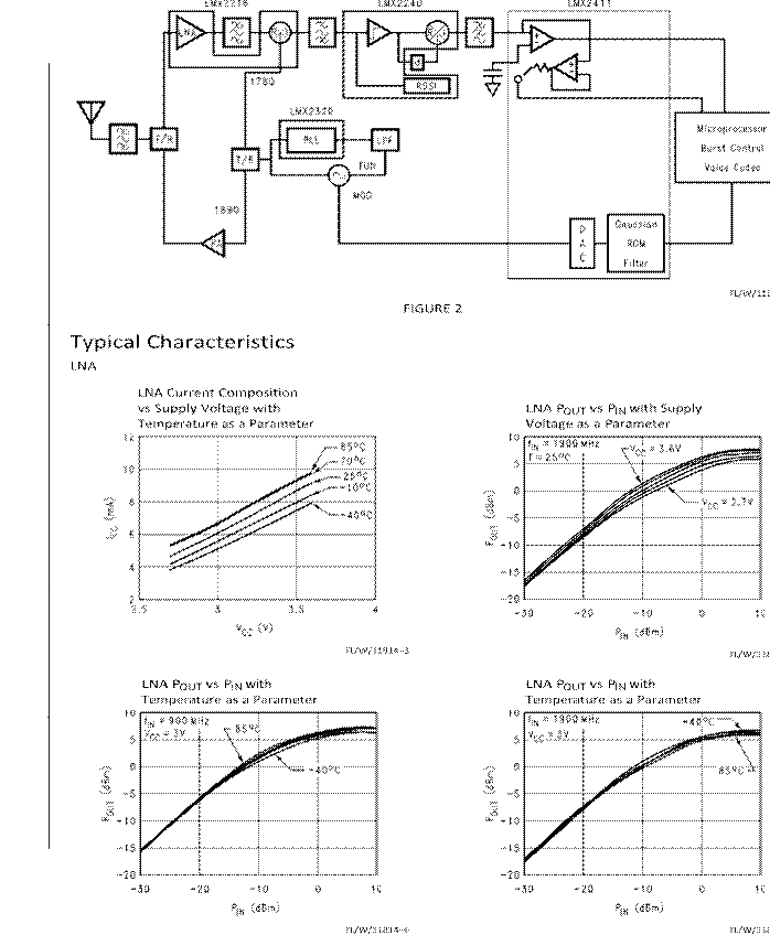
LNA (Continued)
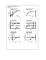
LNA Gain vs Frequency with Supply LNA Noise Figure vs Frequency with
Voltage as a Parameter Supply Voltage as a Parameter
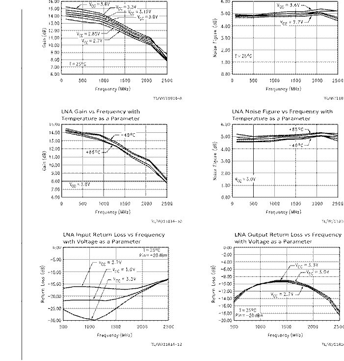
MIXER
Mixer Gain (Double Sideband) Mixer Gain (Double Sideband)
vs Frequency with Supply vs Frequency with Temperature
Voltage as a Parameter as a Parameter
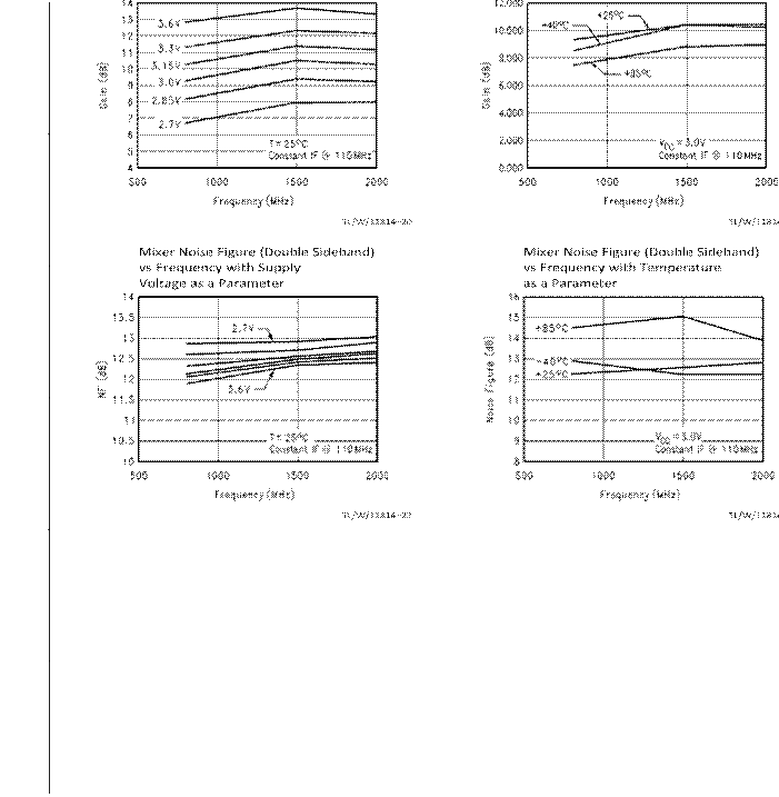
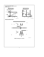
MIXER (Continued)
Mixer POUT vs PIN with Supply Mixer POUT vs PIN with Supply
Voltage as a Parameter Voltage as a Parameter
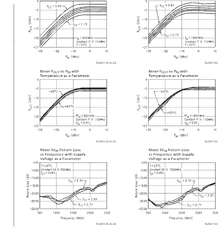
MIXER (Continued)
Mixer RFIN Return Loss vs Frequency with Supply
Voltage as a Parameter
Mixer IFOUT Return Loss vs Frequency with Supply
Voltage as a Parameter
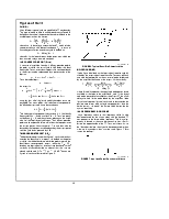
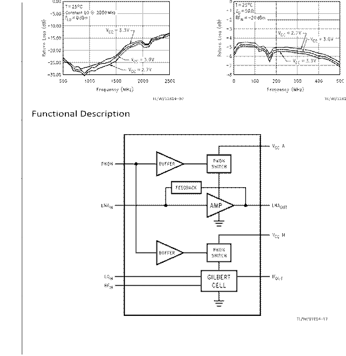 FIGURE 3. Block
Diagram of the LMX2216
FIGURE 3. Block
Diagram of the LMX2216
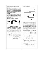
THE LNA
The LNA is a common emitter stage with active feedback. This feedback network allows for wide bandwidth operation while providing the necessary optimal input impedance for low noise performance. The power down feature is implemented using a CMOS buffer and a power-down switch. The power down switch is implemented with CMOS devices. During power down, the switch is open and only leakage currents are drawn from the supply.
THE MIXER
The mixer is a Gilbert cell architecture, with the RF input signal modulating the LO signal and single ended output taken from the collector of one of the upper four transistors. The power down circuitry of the mixer is similar to that of the LNA. The power down switch is used to provide or cut off bias to the Gilbert cell.
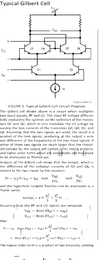
TL/W/11814–14
FIGURE 4. Typical LNA Structure
 A
typical low noise amplifier consists of an active amplifying element and input
and output matching networks. The input matching network is usually optimized
for noise performance, and the output matching network for gain. The active
element is chosen such that it has the lowest optimal noise figure, FMIN, an intrinsic property of
the device. The noise figure of a linear two-port is a function of the source
admittance and can be expressed by
A
typical low noise amplifier consists of an active amplifying element and input
and output matching networks. The input matching network is usually optimized
for noise performance, and the output matching network for gain. The active
element is chosen such that it has the lowest optimal noise figure, FMIN, an intrinsic property of
the device. The noise figure of a linear two-port is a function of the source
admittance and can be expressed by
F e FMIN a Rn [(GON b GG)2 a (BON b BG)2] GG
where GG a jBG e generator admittance presented to the input of the two port,
GON a jBON e generator admittance at which optimum noise figure occurs,
Rn e empirical constant relating the sensitivity of the noise figure to generator admittance.
 )a
)a
a sum of two sinusoids,
AB cos ((0
IEE 2 cos ((RF0RFa0LO0)LOt a) t wRFwRFawLOw)LO) one of which
Уважаемый посетитель!
Чтобы распечатать файл, скачайте его (в формате Word).
Ссылка на скачивание - внизу страницы.