 CA3127
March 1993 High Frequency N-P-N Transistor Array
|
Features Description • Gain Bandwidth Product (fT). . . . . . . . . . . . . . . . >1GHz The CA3127* consists of five general purpose silicon n-p-n transistors on a common monolithic substrate. Each of the • Power Gain. . . . . . . . . . . . . . . . . 30dB (Typ) at 100MHzcompletely isolated transistors exhibits low 1/f noise and a • Noise Figure. . . . . . . . . . . . . . . . 3.5dB (Typ) at 100MHz value of fT in excess of 1GHz, making the CA3127 useful from DC to 500MHz. Access is provided to each of the termi• Five Independent Transistors on a Common Substrate nals for the individual transistors and a separate substrate connection has been provided for maximum application flexiApplications bility. The monolithic construction of the CA3127 provides close electrical and thermal matching of the five transistors. • VHF Amplifiers * Formerly Development Number TA6206. • Multifunction Combinations - RF/Mixer/Oscillator
• Sense Amplifiers Ordering Information
• Synchronous Detectors • VHF Mixers • IF Converter • IF Amplifiers • Synthesizers • Cascade Amplifiers * Denotes Tape and Reel.
Pinout CA3127 (PDIP, CDIP, 150MIL SOIC) TOP VIEW
|
CAUTION: These devices are sensitive to electrostatic discharge. Users should follow proper I.C. Handling Procedures. File Number 662.2
Copyright © Harris Corporation 1993
|
Absolute Maximum Ratings |
Operating Conditions |
|
Power Dissipation, PD Any One Transistor . . . . . . . . . . . . . . . . . . . . . . . . . . . . . 85mW |
Operating Temperature Range . . . . . . . . . . . . . . . . -55oC to +125oC Storage Temperature Range. . . . . . . . . . . . . . . . . . -65oC to +150oC |
Total Package
For TA Up to +75oC . . . . . . . . . . . . . . . . . . . . . . . . . . . . 425mW
For TA > +75oC . . . . . . . . . . . . . .Derate Linearly at 6.67mW/oC The following ratings apply for each transistor in the device
Collector-to-Emitter Voltage, VCEO . . . . . . . . . . . . . . . . . . . . . 15V Collector-to-Base Voltage, VCBO. . . . . . . . . . . . . . . . . . . . . . . 20V Collector-to-Substrate Voltage, VCIO (Note 1). . . . . . . . . . . . . 20V
Collector Current, IC . . . . . . . . . . . . . . . . . . . . . . . . . . . . . . .20mA Junction Temperature. . . . . . . . . . . . . . . . . . . . . . . . . . . . . . +175oC Junction Temperature (Plastic Packages) . . . . . . . . . . . . . . +150oC
Lead Temperature (Soldering 10 Sec.). . . . . . . . . . . . . . . . . +300oC
CAUTION: Stresses above those listed in “Absolute Maximum Ratings” may cause permanent damage to the device. This is a stress only rating and operation of the device at these or any other conditions above those indicated in the operational sections of this specification is not implied.
![]()
Electrical Specifications TA = +25oC
|
PARAMETERS |
TEST CONDITIONS |
LIMITS |
UNITS |
|||
|
MIN |
TYP |
MAX |
||||
|
DC SPECIFICATIONS (For Each Transistor) |
||||||
|
Collector-to-Base Breakdown Voltage |
IC = 10µA, IE = 0 |
20 |
32 |
- |
V |
|
|
Collector-to-Emitter Breakdown Voltage |
IC = 1mA, IB = 0 |
15 |
24 |
- |
V |
|
|
Collector-to-Substrate Breakdown-Voltage |
IC1 = 10µA, IB = 0, IE = 0 |
20 |
60 |
- |
V |
|
|
Emitter-to-Base Breakdown Voltage (Note 2) |
IE = 10µA, IC = 0 |
4 |
5.7 |
- |
V |
|
|
Collector-Cutoff-Current |
VCE = 10V IB = 0 |
- |
- |
0.5 |
µA |
|
|
Collector-Cutoff-Current |
VCB = 10V, IE = 0 |
- |
- |
40 |
nA |
|
|
DC Forward-Current Transfer Ratio |
VCE = 6V |
IC = 5mA |
35 |
88 |
- |
|
|
IC = 1mA |
40 |
90 |
- |
|||
|
IC = 0.1mA |
35 |
85 |
- |
|||
|
Base-to-Emitter Voltage |
VCE = 6V |
IC = 5mA |
0.71 |
0.81 |
0.91 |
V |
|
IC = 1mA |
0.66 |
0.76 |
0.86 |
V |
||
|
IC = 0.1mA |
0.60 |
0.70 |
0.80 |
V |
||
|
Collector-to-Emitter Saturation Voltage |
IC = 10mA, IB = 1mA |
- |
0.26 |
0.50 |
V |
|
|
Magnitude of Difference in VBE |
Q1 & Q2 Matched VCE = 6V, IC = 1mA |
- |
0.5 |
5 |
mV |
|
|
Magnitude of Difference in IB |
- |
0.2 |
3 |
µA |
||
|
SWITCHING SPECIFICATIONS |
||||||
|
Noise Figure |
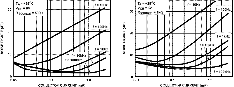
f = 100kHz, RS = 500Ω, IC = 1mA |
- |
2.2 |
- |
dB |
|
|
Gain-Bandwidth Product |
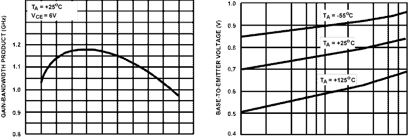
VCE = 6V, IC = 5mA |
- |
1.15 |
- |
GHz |
|
|
Collector-to-Base Capacitance |
VCB = 6V, f = 1MHz |
- |
See Fig. 5 |
- |
pF |
|
|
Collector-to-Substrate Capacitance |
VCI = 6V, f = 1MHz |
- |
- |
pF |
||
|
Emitter-to-Base Capacitance |
VBE = 4V, f = 1MHz |
- |
- |
pF |
||
|
Voltage Gain |
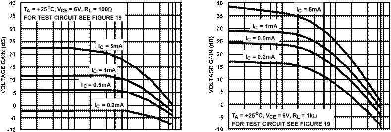
VCE = 6V, f = 10MHz, RL = 1kΩ, IC = 1mA |
- |
28 |
- |
dB |
|
|
Power Gain |
Cascode Configuration f = 100MHz, V+ = 12V, IC = 1mA |
27 |
30 |
- |
dB |
|
|
Noise Figure |
- |
3.5 |
- |
dB |
||
|
Input Resistance |
Common-Emitter Configuration VCE = 6V, IC = 1mA, f = 200 MHz |
- |
400 |
- |
Ω |
|
|
Output Resistance |
- |
4.6 |
- |
kΩ |
||
|
Input Capacitance |
- |
3.7 |
- |
pF |
||
|
Output Capacitance |
- |
2 |
- |
pF |
||
|
Magnitude of Forward Transadmittance |
- |
24 |
- |
mmho |
||
NOTE:
1. The collector of each transistor of the CA3127 is isolated from the substrate by an integral diode. The substrate (terminal 5) must be connected to the most negative point in the external circuit to maintain isolation between transistors and to provide for normal transistor action.
2. When used as a zener for reference voltage, the device must not be subjected to more than 0.1mJ of energy from any possible capacitanceor electrostatic discharge in order to prevent degradation of the junction. Maximum operating zener current should be less than 10mA.
0 1 2 3 4 5 6 7 8 9 10
COLLECTOR CURRENT (mA)
0 1 2 3 4 5 6 7 8 9 10
BIAS VOLTAGE (V)
0.1 1 10
COLLECTOR CURRENT (mA)
|
TRAN- SISTOR |
CAPACITANCE (pF) |
|||||||
|
CCB |
CCE |
CEB |
CCI |
|||||
|
PKG |
TOTAL |
PKG |
TOTAL |
PKG |
TOTAL |
PKG |
TOTAL |
|
|
BIAS (V) |
- |
6V |
- |
6V |
- |
4V |
- |
6V |
|
Q1 |
0.025 |
0.190 |
0.090 |
0.125 |
0.365 |
0.610 |
0.475 |
1.65 |
|
Q2 |
0.015 |
0.170 |
0.225 |
0.265 |
0.130 |
0.360 |
0.085 |
1.35 |
|
Q3 |
0.040 |
0.200 |
0.215 |
0.240 |
0.360 |
0.625 |
0.210 |
1.40 |
|
Q4 |
0.040 |
0.190 |
0.225 |
0.270 |
0.365 |
0.610 |
0.085 |
1.25 |
|
Q5 |
0.010 |
0.165 |
0.095 |
0.115 |
0.140 |
0.365 |
0.090 |
1.35 |
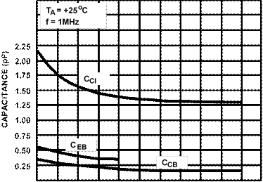
FIGURE 5B. TYPICAL CAPACITANCE VALUES AT f = 1MHz. THREE TERMINAL MEASUREMENT. GUARD ALL TERMINALS EXCEPT THOSE UNDER TEST.
1 10 100 1000 1 10 100 1000
FREQUENCY (MHz) FREQUENCY (MHz)
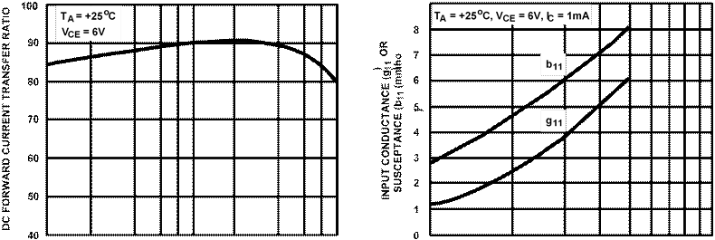
0.1 1.0 10
COLLECTOR CURRENT (mA)
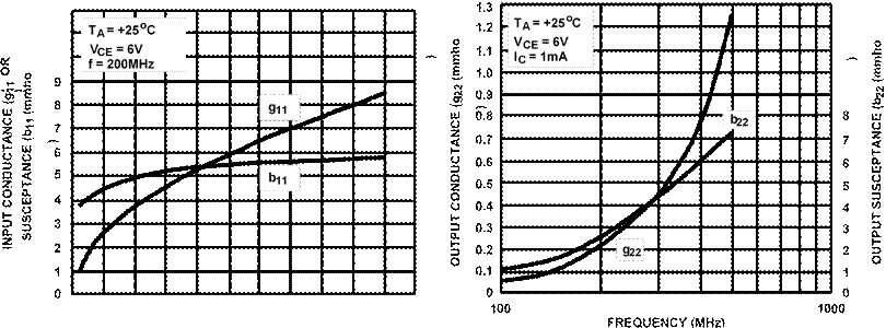 FIGURE 8. DC
FORWARD-CURRENT TRANSFER RATIO (hFE) vs COLLECTOR CURRENT
FIGURE 8. DC
FORWARD-CURRENT TRANSFER RATIO (hFE) vs COLLECTOR CURRENT100 1000
FREQUENCY (MHz)
0 1 2 3 4 5 6 7 8 9 10
COLLECTOR CURRENT (mA)
FIGURE 10. INPUT ADMITTANCE (Y11) vs COLLECTOR CURRENT
0 1 2 3 4 5 6 7 8 9 10 11 12 COLLECTOR CURRENT (mA)
 |
 |
COLLECTOR CURRENT (mA)
100 150 200 1000
FREQUENCY (MHz)
0 1 2 3 4 5 6 7 8 9 10 11 12
COLLECTOR CURRENT (mA)
 |
Уважаемый посетитель!
Чтобы распечатать файл, скачайте его (в формате Word).
Ссылка на скачивание - внизу страницы.