 Simple
Bias Supplies ®
Simple
Bias Supplies ®
Using the TOP200
Power systems often require significant amounts of bias power from a small, separate, regulated power supply. Applications which use bias supplies include computer power supplies, uninterruptible power systems, motor controllers, electric power meters, and appliance controllers. A housekeeping power supply is often required in equipment designed for long periods of low power quiescent operation. The supply provides power for separate circuitry waiting for input. One important application is the “Green PC” which enters a low power sleep mode until awakened by keyboard entry or I/O activity. Fax machines, televisions, VCRs, video monitors, laser printers, and copiers are other applications that often require small housekeeping supplies.
Two common methods for supplying bias power are linear supplies utilizing a line frequency transformer or switching power supplies using a blocking oscillator circuit. These approaches can encounter difficulties when wide range input, high efficiency, and/or small size is required. Using TOPSwitch®, a primary regulated switching power supply can be constructed that approaches the simplicity of a linear design, but with wide range input, good efficiency, and very small size and weight.
For the sake of clarity, the following application circuits will assume an AC input voltage has been rectified and filtered elsewhere in the system such that high voltage DC is available. If the circuit is located far away from the bulk high-voltage supply, a decoupling capacitor of 0.1 to 1 µF is recommended across the high-voltage input. This capacitor should be placed so that it is close to U1 and T1, and the loop between the decoupling capacitor, U1, and T1 is as small as possible.
The circuit descriptions below assume some familiarity with the functioning of TOPSwitch. For greater detail on the TOPSwitch integrated circuit, please refer to the data sheets for TOP100-4 and TOP200-4, as well as AN-14.
|
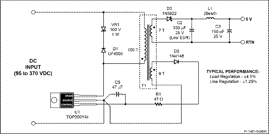
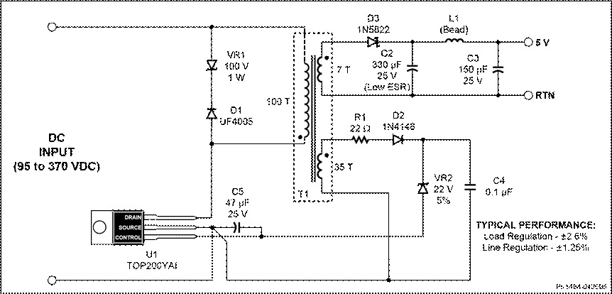
Figure 1. Minimum Part Count Bias Supply Using the TOP200.
December 1995 |
The circuits shown in Figures 1 and 2 are simple 5 V, 5 watt bias supplies using the TOP200. Both circuits are full-range input flyback power supplies that employ primary-side regulation from a transformer bias winding. This approach is best for lowcost applications requiring isolation and operation within a narrow range of load power. Line and load regulation of ±5%
 |
or better can be achieved from 10% to 100% of rated load. Careful attention is required in transformer construction and layout to reduce the effects of stray inductance.
Voltage feedback in both circuits is obtained from the transformer bias winding, which eliminates the need for optocouplers and secondary-referenced error amplifiers. High-voltage DC is applied to the primary winding of T1. The other side of the transformer primary is driven by the integrated high-voltage MOSFET transistor within the TOP200 (U1). Both circuits operate at a switching frequency of 100 kHz, set by the internal oscillator of the TOP200. The clamp circuit implemented by VR1 and D1 limits the leading-edge voltage spike caused by transformer leakage inductance to a safe value. The 5 V power secondary winding is rectified and filtered by D3, C2, C3, and L1 to create the 5 V output voltage.
The circuits in Figures 1 and 2 differ only in the manner in which voltage feedback from the bias winding is used to control the output voltage. In the circuit of Figure 1, the output of the T1 bias winding is rectified and filtered by R1, D2, and C5. The voltage across C5 is regulated by U1, and is determined by the voltage drop across the 5.7 V internal shunt regulator at the CONTROL pin of U1. A voltage on C5 greater than the drop across the CONTROL pin of U1 will cause current to flow into the CONTROL pin of U1. The operating duty cycle is inversely proportional to the control current, with the result that U1 will adjust its duty cycle to minimize the control current to a value that maintains the 5.7 V control voltage. The output voltage of the bias winding is reflected by the turns ratio between the bias winding and the output winding to determine the output voltage. C5 is used to bypass the CONTROL pin of U1. It also provides loop compensation for the power supply by shunting AC currents around the CONTROL pin, and also determines the auto-restart frequency of U1 during start-up and short circuit conditions. See the TOP100-4 or TOP200-4 data sheets for more detail on these functions.
The circuit of Figure 2 is slightly more complex, and should be used when tighter load regulation is required. C4 and VR2 have been added, and the supply is now regulated by the combination of the internal 5.7 V shunt regulator at the CONTROL pin of U1 and the voltage drop across VR2.
Уважаемый посетитель!
Чтобы распечатать файл, скачайте его (в формате Word).
Ссылка на скачивание - внизу страницы.