|
Design Idea DI-10®
INTEGRATIONS, INC. PC Standby |
||||||
|
Application |
Device |
Power Output |
Input Voltage |
Output Voltage |
Topology |
|
|
PC Standby |
TOP232Y |
17 W |
200 - 375 VDC |
3.3 V / 5 V |
Flyback |
|
|
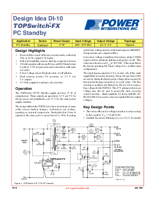
Design Highlights current and voltage stresses on the internal power MOSFET, clamp circuits and output rectifier. • Exceeds Blue Angel efficiency requirements, achieving Line under-voltage is implemented using a single 3.9 MΩ 78% at 3.9 W output (5 W input) resistor (R1) to eliminate glitches during turn-on/off. This • Soft-start capability reduces start-up component stresses value was chosen to set V at 195 VDC. This is just below • 132 kHz operation allow small, low cost EE19 transformer UV the lowest operating DC input voltage for a doubler input to deliver 17 W and prevents audio interaction with main configuration. converter • Under-voltage detect eliminates turn-on/off glitches The input bypass capacitor C1 is needed only if the main • Dual sensing ensures 5% accuracy on 3.3 V and supply filter is located remotely. Diode D1 and Zener VR1 5 V outputs are used to clamp the leading edge voltage spikes caused by • 15 V bias supply for primary side circuitry transformer leakage inductance, to a safe value. The bias winding is rectified and filtered by D2 and C6 to create a Operation bias voltage for the TOP232. This 15 V primary referenced voltage may also be used to power the main converter The TOPSwitch-FX PC Standby supply provides 17 W of control circuitry. Shunt regulator U3 along with R6, R7, output power. Three outputs are generated, 3.3 V and 5 V for R9, R10 & R11 are used to sense and regulate the two output the processor and peripherals, and 15 V for the main power voltages. supply switcher. The design utilizes the TOP232 and takes advantage of many Key Design Points of the device's built in features. Soft-start is one of these, • The value of the under-voltage detection is set according requiring no external components. During the first 10 ms of operation, the duty cycle is raised from 0 to 78%, lowering to the equation VUV = 50 µA x R1.
* Optional PI-2537-071200 Figure 1. TOPSwitch-FX 17 W PC Standby |
||||||
DI-10 www.powerint.com July 2001
DI-10
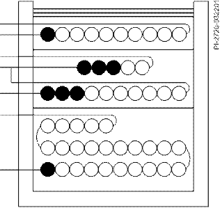
in low output ripple on 3.3 V and 5 V channels. At full load, peak-to-peak ripple is significantly below 50 mV. • Y1 capacitor (CY1) is tied between secondary return and primary positive DC rail to minimize potential noise coupling to SOURCE pin during AC common mode surge events. • Good cross regulation on the main channels is maximized with dual sense feedback to the 3.3 V and 5 V outputs (R9, R10). • Capacitor (C8) is added to eliminate output start-up overshoot on DC output channels. • Feedback compensation is accomplished with capacitor C7, across TL431 reference amplifier (U3), and correct choice of CONTROL pin capacitor and series resistor (C5, R5). Resistor R6 sets feedback gain while resistor R7 provides bias to the TL431 when the 5 V output is lightly loaded. Compensation is optimized for the transformer design and the power supply provides satisfactory phase margin and operating bandwidth across wide operating conditions. Table 1. Transformer construction information
0 50 100 Time ( s) Figure 2. DC output ripple seen on +3.3 V output, full load Figure 3. Transformer build diagram For the latest updates, visit our Web site: www.powerint.com Power Integrations reserves the right to make changes to its products at any time to improve reliability or manufacturability. Power Integrations does not assume any liability arising from the use of any device or circuit described herein, nor does it convey any license under its patent rights or the rights of others. The PI Logo, TOPSwitch, TinySwitch and EcoSmart are registered trademarks of Power Integrations, Inc. ©Copyright 2001, Power Integrations, Inc.
WORLD HEADQUARTERS EUROPE & AFRICA TAIWAN CHINA AMERICAS Power Integrations (Europe) Ltd. Power Integrations Power Integrations Power Integrations, Inc. United Kingdom International Holdings, Inc. International Holdings, Inc. San Jose, CA 95138 USA Phone: +44-1344-462-300 Taipei, Taiwan China Customer Service: Fax: +44-1344-311-732 Phone: +886-2-2727-1221 Phone: +86-755-367-5143 Phone: +1 408-414-9665 e-mail: eurosales@powerint.com Fax: +886-2-2727-1223 Fax: +86-755-377-9610 Fax: +1 408-414-9765 e-mail: taiwansales@powerint.com e-mail: chinasales@powerint.com e-mail: usasales@powerint.com KOREA JAPAN INDIA (Technical Support) APPLICATIONS HOTLINE Power Integrations Power Integrations, K.K. Innovatech World Wide +1-408-414-9660 International Holdings, Inc. Keihin-Tatemono 1st Bldg. Bangalore, India Seoul, Korea Japan Phone: +91-80-226-6023 APPLICATIONS | ||||||||||||||||
Уважаемый посетитель!
Чтобы распечатать файл, скачайте его (в формате Word).
Ссылка на скачивание - внизу страницы.

 TOPSwitch-FX® POWER
 • Suitable
layout and filtering (L1, L2, C11, C13) results
• Suitable
layout and filtering (L1, L2, C11, C13) results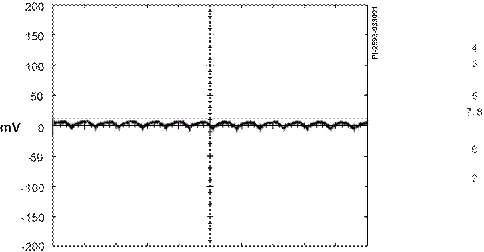
 1
1