
|
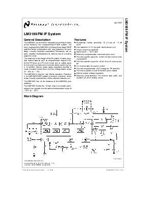
LM3189 FM IF System General Description Features The LM3189N is a monolithic integrated circuit that provides Y Exceptional limiting sensitivity: 12 mV typ at b3 dB all the functions of a comprehensive FM IF system. The point block diagram of the LM3189N includes a three stage FM IF Y Low distortion: 0.1% typ (with double-tuned coil) amplifier/limiter configuration with level detectors for each Y Single-coil tuning capability stage, a doubly balanced quadrature FM detector and an Y Improved (S a N)/N ratio audio amplifier that features the optional use of a muting Y Externally programmable recovered audio level (squelch) circuit. Y Provides specific signal for control of inter-channel mutThe advanced circuit design of the IF system includes desir- ing (squelch) able deluxe features such as programmable delayed AGC Y Provides specific signal for direct drive of a tuning mefor the RF tuner, an AFC drive circuit, and an output signal ter to drive a tuning meter and/or provide stereo switching logY On channel step for search control ic. In addition, internal power supply regulators maintain a Y Provides programmable AGC voltage for RF amplifier nearly constant current drain over the voltage supply range of a8.5V to a16V. Y Provides a specific circuit for flexible audio output Y Internal supply voltage regulators The LM3189N is ideal for high fidelity operation. Distortion in an LM3189N FM IF system is primarily a function of the Y Externally programmable ON channel step width, and phase linearity characteristic of the outboard detector coil. deviation at which muting occurs The LM3189N has all the features of the LM3089N plus additions. The LM3189N utilizes the 16-lead dual-in-line plastic package and can operate over the ambient temperature range of b40§C to a85§C. |
|
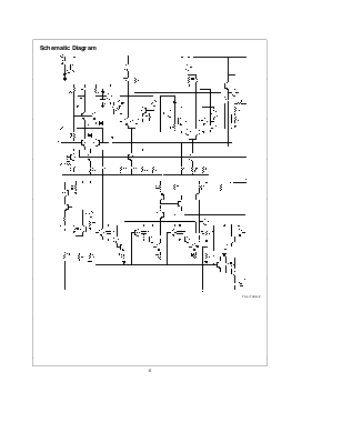
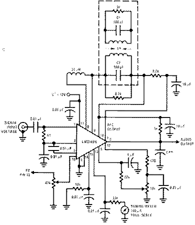
Block Diagram
TL/H/7960–1 All resistance values are in X *L tunes with 100 pF (C) at 10.7 MHz, Q0 j 75 (Toko No. KACS K586HM or equivalent) |
|
Absolute Maximum Ratings If Military/Aerospace specified devices are required, Power Dissipation (Note 2) 1500 mW please contact the National Semiconductor Sales Operating Temperature Range b40§C to a85§C Office/Distributors for availability and specifications. Storage Temperature Range b65§C to a150§C Supply Voltage Between Pin 11 and Pins 4, 14 16V Lead Temperature (Soldering, 10 sec.) 260§C DC Current Out of Pin 12 5 mA DC Current Out of Pin 13 5 mA DC Current Out of Pin 15 2 mA Electrical Characteristics TA e 25§C, Vae 12V |
|||||||
|
Symbol |
Parameter |
Conditions (See Single-Tuned Test Circuit) |
Min |
Typ |
Max |
Units |
|
|
STATIC (DC) CHARACTERISTICS |
|||||||
|
I11 |
Quiescent Circuit Current |
20 |
31 |
44 |
mA |
||
|
DC Voltages: |
|||||||
|
V1 |
Terminal 1 (IF Input) |
1.2 |
2.0 |
2.4 |
V |
||
|
V2 |
Terminal 2 (AC Return to Input) |
No Signal Input, Non Muted |
1.2 |
2.0 |
2.4 |
V |
|
|
V3 |
Terminal 3 (DC Bias to Input) |
1.2 |
2.0 |
2.4 |
V |
||
|
V15 |
Terminal 15 (RF AGC) |
7.5 |
9.5 |
11 |
V |
||
|
V10 |
Terminal 10 (DC Reference) |
5 |
5.75 |
6 |
V |
||
|
DYNAMIC CHARACTERISTICS |
|||||||
|
VI(lim) |
Input Limiting Voltage (b3 dB Point) |
fo e 10.7 MHz, |
12 |
25 |
mV |
||
|
AMR |
AM Rejection (Term. 6) |
VIN e 0.1V AM Mod. e 30% |
45 |
55 |
dB |
||
|
VO(AF) |
Recovered AF Voltage (Term. 6) |
325 |
500 |
650 |
mV |
||
|
THD |
Total Harmonic Distortion (Note 1) |
fmod e 400 Hz, |
|||||
|
Single Tuned (Term. 6) |
Deviation g75 kHz |
0.5 |
1 |
% |
|||
|
Double Tuned (Term. 6) |
VIN e 0.1V |
0.1 |
% |
||||
|
S a N/N |
Signal Plus Noise to Noise Ratio (Term. 6) |
65 |
80 |
dB |
|||
|
fDEV |
Deviation Mute Frequency |
fmod e 0 |
g40 |
kHz |
|||
|
V16 |
RF AGC Threshold |
1.25 |
V |
||||
|
V12 |
On Channel Step |
VIN e 0.1V |
fDEV kg40 kHz fDEV lg40 kHz |
0 5.6 |
V |
||
|
Note 1: THD characteristics are essentially a function of the phase characteristics of the network connected between terminals 8, 9, and 10. Note 2: For operation in ambient temperatures above 25§C, the device must be derated based on a 150§C maximum junction temperature and a thermal resistance of 80§C/W junction to ambient. Connection Diagram Dual-In-Line Package
TL/H/7960–2 Top View Order Number LM3189N See NS Package Number N16E |
|||||||
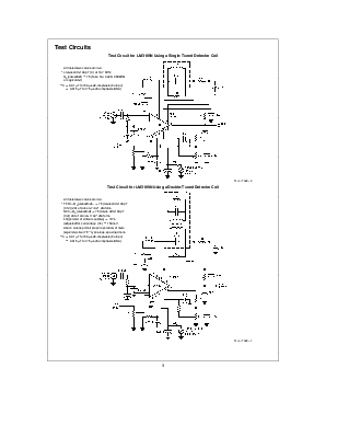
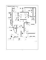
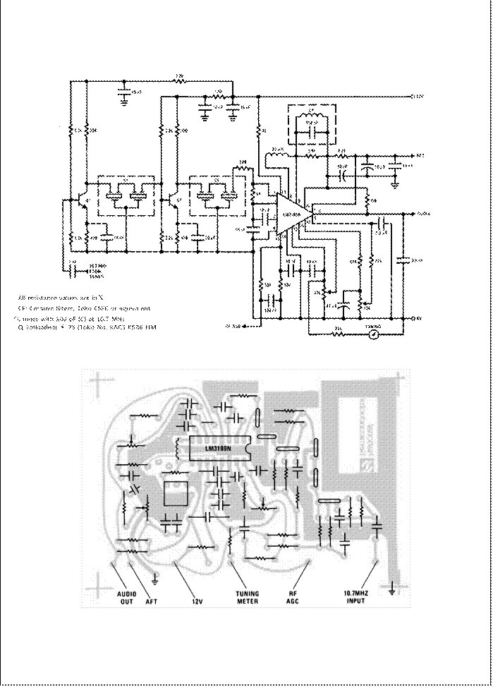
Test Circuit for LM3189N Using a Single-Tuned Detector Coil

![]()
 All resistance values are in X
*L tunes with 100 pF (C) at 10.7 MHz, Qo(unloaded) j 75 (Toko No. KACS K586HM or equivalent)
**C e0.01 mF for 50 ms de-emphasis (Europe) e 0.015 mF for 75 ms de-emphasis (USA)
![]() Test Circuit for LM3189N Using a Double-Tuned
Detector Coil
Test Circuit for LM3189N Using a Double-Tuned
Detector Coil
All resistance values are in X
*T:PRIÐQo(unloadedÐ j 75 (tunes with 100 pF
(C12)) 20t of 34e on 7/32× dia form
SECÐQo(unloaded) j 75 (tunes with 100 pF (C2)) 20t of 34e on 7/32× dia form kQ(percent of critical coupling) j 70% (adjusted for coil voltage (V ) e 150 mV
Above values permit proper operation of mute
(squelch) circuit ‘‘E’’ type slugs, spacing 4 mm
**C e0.01 mF for 50 ms de-emphasis (Europe) e 0.015 mF for 75 ms de-emphasis (USA)
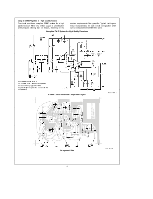
 Complete FM IF System for High Quality
Tuners
Complete FM IF System for High Quality
Tuners
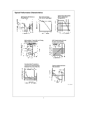
The circuit provides a complete FM IF system for a high receiver requirements. See graph for Typical Limiting and quality receiver. Either one or two stages of amplification Noise Characteristics
Уважаемый посетитель!
Чтобы распечатать файл, скачайте его (в формате Word).
Ссылка на скачивание - внизу страницы.

