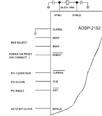
The ADSP-2192 processor can also be operated with an external frequency generator or integrated oscillator supplying the clock signal. If an external clock is used, the input should be connected to the XTALI pin, and the XTALO pin must be left unconnected. If the input waveform exceeds a 2.5V signal level, the CLKSEL pin should be tied to VBYP (2.5V) to protect the internal oscillator. The XTALI signal may not be halted, changed, or operated below the specified frequency during normal operation.
The internal phase locked loop (PLL) of the processors generates an internal clock that is, by default, six times the input frequency. This clock rate is configurable, and the multiplier’s default value of six can be changed, according to the bit settings of DPLLN, DPLLK, and DPLLM in the DSP’s PLL control register.
C loc k Sig na ls
For more information about the programmable PLL, see “Setting Dual DSP Core Features” on page 6-3.

Figure 11-1. External Crystal Connections
The ADSP-2192 defines the following clock domains: PCI, USB, AC’97, DSP clock, and the Peripheral Device Control (PDC) bus. Figure 11-2 on page 11-9 shows these clock domains and their relationships to each other.

Figure 11-2. ADSP-2192 Clock Domains
Each peripheral has several asynchronous inputs (interrupt requests, for example), which can be asserted in arbitrary phase to the processor clock. The processor synchronizes such signals before recognizing them. The delay associated with signal recognition is called synchronization delay.
Different asynchronous inputs are recognized at different points in the processor cycle. Any asynchronous input must be valid prior to the recognition point to be recognized in a particular cycle. If an input does not meet the setup time on a given cycle, it is recognized either in the current cycle or during the next cycle if it remains valid.
C loc k Sig na ls
Edge-sensitive interrupt requests are latched internally so that the request signal only has to meet the pulse width requirement. To ensure the recognition of any asynchronous input, however, the input must be asserted for at least one full processor cycle plus setup and hold time. Setup and hold times are specified in the data sheet for the ADSP-2192 or data sheets for other products in the ADSP-219x family.
The processors on the ADSP-2192 use an on-chip phase-locked loop (PLL) to generate the internal clock signals. Because these clocks are generated based on the rising edge of XTALI, there is no ambiguity about the phase relationship of two processors sharing the same input clock. Multiple processor synchronization is simplified as a result.
Using an input clock
with more than one possible frequency (with the phase-locked loop generating
the internal clock cycles, based on the configurable value of the clock
multiplier) imposes certain restrictions. The XTALI signal must be valid
long enough to achieve phase lock before PORST![]() can be
deasserted. Also, the clock input frequency cannot be changed unless the
processor is in PORST
can be
deasserted. Also, the clock input frequency cannot be changed unless the
processor is in PORST![]() .
.
The PLLCTL register controls clock multiplier modes for the ADSP-2192. See “ADSP-2192 DSP Peripheral Registers” on page B-1 for more information about the bits in PLLCTL. These modes affect operations for both DSP cores. See “Clock Multiplier Mode Control” on page 6-10 for more instructions on how to change the clock multiplier.
When writing DSP algorithms, you can significantly improve performance by executing many instructions in parallel, or within the same clock cycle. This is called parallel operation, and the instructions that execute multiple operations within a single cycle are called multifunction instructions.
Уважаемый посетитель!
Чтобы распечатать файл, скачайте его (в формате Word).
Ссылка на скачивание - внизу страницы.