Arbitration for accesses to shared memory is fixed with the highest priority for DSP P0 and the lowest priority for DSP P1.
Each DAG is associated with a particular data bus and memory page. From settings at reset, DAG1 supplies addresses over the DM bus for memory page 0 and DAG2 supplies addresses over the PM bus for memory page 0. These selections can be changed using the DMPGx registers. For more information on address generation, see “Program Sequencer” on page 3-1 or “Data Address Generators” on page 4-1.
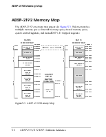
*N O TE: EA C H M EM O RY BLO C K HA S A S EPA RA TE C O N N EC TIO N TO THE PM A N D D M BUS ES.
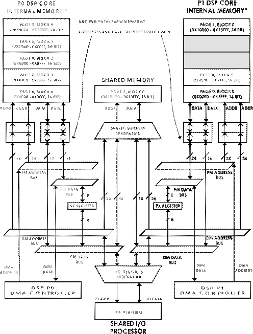
Figure 5-1. ADSP-2192 Memory and Internal Buses Block Diagram Because the DSP’s blocks of internal memory have different widths, placing 16-bit data in a Program Memory block leaves some space unused. For more information on how the DSP works with memory words, see “P0 DSP Core Internal Memory Space” on page 5-10.
The PM data bus is 24 bits wide, and the DM data bus is 16 bits wide. Both data buses can handle data words (16-bit), but only the PM data bus carries instruction words (24-bit).
The data buses let programs transfer the contents of one register to another or to any internal memory location in a single cycle. As shown in Figure 5-1, the PM Bus Exchange (PX) register permits data to flow between the PM and DM data buses. The PX register holds the lower 8 bits during transfers between the PM and DM buses. The alignment of PX register to the buses appears in Figure 5-2.
23 0
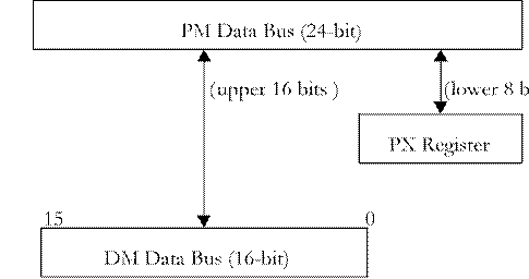
Figure 5-2. PM Bus Exchange (PX) Registers
The PX register is a Register Group 3 (REG3) registers and is accessible for register-to-register transfers.
|
! |
When reading data from program memory and data memory simultaneously, there is a dedicated path from the upper 16 bits of the PM data bus to the Y registers of the computational units. This read-only path does not use the bus exchange circuit.
For transferring data from the PM data bus, the PX register is:
1. Loaded automatically whenever data (not an instruction) is read from program memory to any register. For example:
In this example, the upper 16 bits of a 24-bit program memory word are loaded into AX0 and the lower 8 bits are automatically loaded into PX.
2. Read out automatically as the lower 8 bits when data is written to program memory. For example:
In this example, the 16 bits of AX0 are stored into the upper 16 bits of a 24-bit program memory word. The 8 bits of PX are automatically stored to the 8 lower bits of the memory word.
For transferring data from the DM data bus, the PX register may be:
1. Loaded with a data move instruction, explicitly specifying the PX register as the destination. The lower 8 bits of the data value are used and the upper 8 are discarded.
2. Read with a data move instruction, explicitly specifying the PX register as a source. The upper 8 bits of the value read from the register are all zeroes.
Whenever any register is written out to program memory, the source register supplies the upper 16 bits. The contents of the PX register are added as the lower 8 bits for instructions (such as the Type-1 and Type-32) that use the PX register, but the PX register is not used for other instructions (such as the Type-4, Type-12, and Type-29). If these lower 8 bits of data to be transferred to program memory
Уважаемый посетитель!
Чтобы распечатать файл, скачайте его (в формате Word).
Ссылка на скачивание - внизу страницы.