1 INTRODUCTION
Figure 1-0.
Table 1-0.
Listing 1-0.
The ADSP-219x/2192 DSP Hardware Reference provides architectural information on the ADSP-219x modified Harvard architecture Digital Signal Processor (DSP) core and ADSP-2192 DSP product. The architectural descriptions cover functional blocks, buses, and ports, including all features and processes they support. For programming information, see the ADSP-219x DSP Instruction Set Reference.
DSP system designers and programmers who are familiar with signal processing concepts are the primary audience for this manual. This manual assumes that the audience has a working knowledge of microcomputer technology and DSP-related mathematics.
DSP system designers and programmers who are unfamiliar with signal processing can use this manual, but they should supplement this manual with other texts that describe DSP techniques.
All readers, particularly system designers, should refer to the DSP’s data sheet for timing, electrical, and package specifications. For additional suggested reading, see “For More Information About Analog Products” on page 1-23.
O ve rvie w—Why Fixe d-Point DSP?
O ve rvie w—Why Fix e d -Point DSP?
A digital signal processor’s data format determines its ability to handle signals of differing precision, dynamic range, and signal-to-noise ratios. Because 16-bit, fixed-point DSP math is required for certain DSP coding algorithms, using a 16-bit, fixed-point DSP can provide all the features needed for certain algorithm and software development efforts. Also, a narrower bus width (16-bit as opposed to 32- or 64-bit wide) leads to reduced power consumption and other design savings. The extent to which this is true depends on the fixed-point processor’s architecture. High-level language programmability, large address spaces, and wide dynamic range allow system development time to be spent on algorithms and signal processing concerns, rather than assembly language coding, code paging, and error handling. The ADSP-2192 DSP is a highly integrated, 16-bit fixed-point DSP that provides many of these design advantages.
The ADSP-219x family DSPs are high-performance 16-bit DSPs for communications, instrumentation, industrial/control, voice/speech, medical, military, and other applications. These DSPs provide a DSP core that is compatible with previous ADSP-2100 family DSPs, but they also provide many additional features. The ADSP-219x core combines with on-chip peripherals to form a complete system-on-a-chip. The off-core peripherals add on-chip SRAM, integrated I/O peripherals, timer, and interrupt controller.
The ADSP-219x architecture balances a high performance processor core with high performance buses (PM, DM, DMA). In the core, every computational instruction can execute in a single cycle. The buses and instruction cache provide rapid, unimpeded data flow to the core to maintain the execution rate.
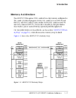
Figure 1-1 shows a detailed block diagram of the ADSP-2192 processor, illustrating the following architectural features:
• Computation units for the ADSP-219x family—multiplier, ALU, shifter, and data register file
• Program sequencer for the ADSP-219x family, with related instruction cache, interval timer, and Data Address Generators (DAG1 and
DAG2)
• PCI/USB Host port
• AC’97 codec port
• SRAM for the ADSP-2192
• Input/Output (I/O) processor with integrated DMA controllers
• JTAG Test Access Port for board test and emulation on the ADSP-2192
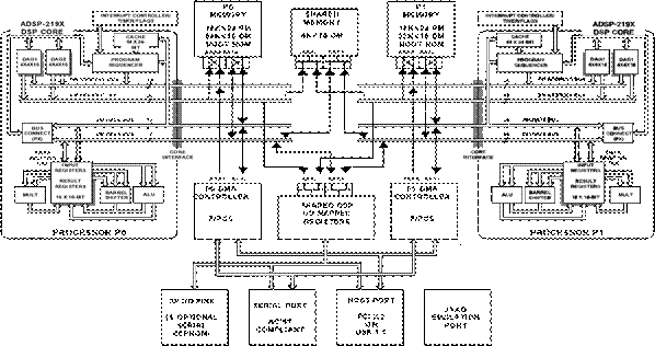
Figure 1-1. ADSP-2192 Block Diagram
Figure 1-1 also shows the two cores of the ADSP-2192 (processors P0 and P1). Additionally, it shows the four on-chip buses of the ADSP-2192:
Уважаемый посетитель!
Чтобы распечатать файл, скачайте его (в формате Word).
Ссылка на скачивание - внизу страницы.