Write to PFDATA sets pin value and may cause interrupt
(level- or edge-sensitive)
• Read of PFDATA gives set value
After reset, the PF pins default to inputs and the interrupts are disabled by the IMASK register’s default value. The pins can be used as PF outputs by changing the PFTYPE register and leaving the interrupt disabled in IMASK. If the pins are to be used as interrupts, then the PFTYPE register need not be changed, but the interrupt must be enabled in the IMASK register.
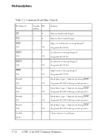
Table 7-3 provides a description of the pins that are common to both Full Memory Mode and Host Memory Mode in 100-LQFP packages. In cases where pin functionality is reconfigurable, the default state is shown in plain text; alternate functionality is shown in italics. All pin descriptions also apply to the processors in 144-Ball Mini-BGA packages unless otherwise noted.
Table 7-3. Common-Mode Pins
|
Pin Name(s) |
Number of Pins |
I/O |
Function |
|
RESET |
1 |
I |
Processor Reset Input |
|
BR |
1 |
I |
Bus Request Input |
|
BG |
1 |
O |
Bus Grant Output |
|
BGH |
1 |
O |
Bus Grant Hung Output |
|
DMS |
1 |
O |
Data Memory Select Output |
|
PMS |
1 |
O |
Program Memory Select Output |
|
IOMS |
1 |
O |
Memory Select Output |
|
BMS |
1 |
O |
Byte Memory Select Output |
|
CMS |
1 |
O |
Combined Memory Select Output |
Table 7-3. Common-Mode Pins (Cont’d)
|
Pin Name(s) |
Number of Pins |
I/O |
Function |
|
RD |
1 |
O |
Memory Read Enable Output |
|
WR |
1 |
O |
Memory Write Enable Output |
|
IRQ2 PF7 |
1 |
I I/O |
Edge- or Level-Sensitive Interrupt Request1 Programmable I/O Pin |
|
IRQL1 PF6 |
1 |
I I/O |
Level-Sensitive Interrupt Requests1 Programmable I/O Pin |
|
IRQL0 PF5 |
1 |
I I/O |
Level-Sensitive Interrupt Requests1 Programmable I/O Pin |
|
IRQE PF4 |
1 |
I I/O |
Edge-Sensitive Interrupt Requests1 Programmable I/O Pin |
|
Mode D PF3 |
1 |
I I/O |
Mode Select Input - Checked only during RESET Programmable I/O Pin during normal operation |
|
Mode C PF2 |
1 |
I I/O |
Mode Select Input - Checked only during RESET Programmable I/O Pin during normal operation |
|
Mode B PF1 |
1 |
I I/O |
Mode Select Input - Checked only during RESET Programmable I/O Pin during normal operation |
|
Mode A PF0 |
1 |
I I/O |
Mode Select Input - Checked only during RESET Programmable I/O Pin during normal operation |
|
CLKIN XTAL |
2 |
I |
Clock or Quartz Crystal Input |
Table 7-3. Common-Mode Pins (Cont’d)
|
Pin Name(s) |
Number of Pins |
I/O |
Function |
|
CLKOUT |
1 |
O |
Processor Clock Output |
|
SPORT0 |
5 |
I/O |
Serial Port I/O Pins |
|
SPORT1
IRQ1:0, FI, FO |
5 |
I/O |
Serial Port I/O Pins Edge- or Level-Sensitive Interrupts, Flag In, Flag Out2 |
|
PWD PWDACK FL0, FL1, FL2 |
1 I 3 |
I O O |
Powerdown Control Input Powerdown Control Output Output Flags |
|
VDD GND (Applies to all ADSP ADSP-2186L, ADSP |
6 10 -2184, AD -2187L pr |
I I SP-2184L, ocessors in |
Power Ground ADSP-2185, ADSP-2185L, ADSP-2186, 100-Lead LQFP package only) |
|
VDD GND (Applies to ADSP- 2 package only) |
11 20 185L, ADS |
I I P-2186, an |
Power Ground d ADSP- 2186L processors in 144-Mini-BGA |
|
VDDINT VDDEXT GND ( |
2 4 10 |
I I I |
Internal VDD (2.5V) Power External VDD (2.5V or 3.3V) Power Ground Applies to all ADSP-218x M and N series processors in 100-Lead LQFP package only) |
Table 7-3. Common-Mode Pins (Cont’d)
|
Pin Name(s) |
Number of Pins |
I/O |
Function |
|
VDDINT VDDEXT GND (Applies to all ADSP |
4 7 20 -218x M a |
I I I nd N series |
Internal VDD (2.5V) Power External VDD (2.5V or 3.3V) Power Ground processors in 144-Ball Mini-BGA package only) |
|
EZ-Port |
9 |
I/O |
For emulation use |
1 Interrupt/Flag Pins retain both functions concurrently. If IMASK is set to enable the corresponding interrupts, then the DSP will vector to the appropriate interrupt vector address when the pin is asserted, either by external devices, or set as a programmable flag.
2 SPORT configuration determined by the DSP System Control register. Software configurable.
Table 7-4 provides a description of Full Memory Mode pins and Table 7-5 provides a description of the Host Memory Mode pins on ADSP-218x processors in 100-lead LQFP and 144-MBGA packages.
Table 7-4. Full Memory Mode Pins (Mode C = 0)
|
Pin Name |
Number of Pins |
I/O |
Function |
|
A13:0 |
14 |
O |
Address Output Pins for Program, Data, Byte and I/O Spaces |
|
D23:0 |
24 |
I/O |
Data I/O Pins for Program, Data, Byte and I/O Spaces (8 MSBs are also used as Byte Memory addresses) |
Table 7-5. Host Memory Mode Pins (Mode C = 1)
|
Pin Name |
Number of Pins |
I/O |
Function |
|
IAD15:0 |
16 |
I/O |
IDMA Port Address/Data Bus |
|
A0 |
1 |
O |
Address Pin for External I/O, Program, Data, or Byte access1 |
|
D23:8 |
16 |
I/O |
Data I/O Pins for Program, Data Byte and I/O spaces |
|
IWR |
1 |
I |
IDMA Write Enable |
|
IRD |
1 |
I |
IDMA Read Enable |
|
IAL |
1 |
I |
IDMA Address Latch Pin |
|
IS |
1 |
I |
IDMA Select |
|
IACK |
1 |
O |
IDMA Port Acknowledge Configurable in Mode D; Open Drain |
![]()
1 In Host Mode, external peripheral addresses can be decoded using the A0, CMS, PMS,
![]()
DMS, and IOMS signals.
To decrease the package size of
the ADSP-218x family processors for the 100-LQFP packages, the IDMA bus and
associated control signals are multiplexed with the external Address and Data
busses. The logic value of the Mode pins are latched on the rising edge of the R![]() ESET
signal. The values of the Mode pins determine whether the DSP will boot from an
EPROM or be booted from an external host processor.
ESET
signal. The values of the Mode pins determine whether the DSP will boot from an
EPROM or be booted from an external host processor.
The Mode pins also determine whether the DSP’s external pins are used for IDMA accesses (Host Memory mode) or whether the full 14-bit address bus and 24-bit data bus is active (Full Memory mode).
The Mode pins can be set for active or passive configuration. An active configuration means that the Mode pin is used as a Mode pin during reset, but also functions alternately as a Programmable Flag pin or Interrupt Signal during runtime. Passive configuration means that the Mode pin is used only as a Mode pin and has no alternate function during runtime.
A passive configuration is more easily implemented because only a simple pullup or pulldown resistor is needed to maintain a proper logic level for the Mode pin. (Tying a Mode pin directly to VDD or GND is also acceptable.)
An Active configuration requires either a weak pullup or pulldown (on the order of 100 kΩ) or some type of tristate driver or logic gate to allow for proper operation of the pin during its alternate mode of functioning as a Programmable Flag pin or Interrupt signal. (A weak pullup or pulldown resistor is used to reduce the amount of current flow to the input pin of the DSP and to minimize the amount of current going through an output driver.) For more information on setting the Mode pins for an active or passive configuration, please see “Using Mode Pins with RESET and ERESET Signals” on page 7-64.
Table 7-6 shows the recommendations for terminating unused pins. Additional recommendations follow the table.
|
! |
Table 7-6 shows the multiplexed pins for the Host Memory mode
Уважаемый посетитель!
Чтобы распечатать файл, скачайте его (в формате Word).
Ссылка на скачивание - внизу страницы.