4 DATA ADDRESS GENERATORS
Figure 4-0.
Table 4-0.
Listing 4-0.
This chapter describes the units that control the movement of data to and from the processor and from one data bus to another within the processor. These units include the following:
• Data address generators (DAGs)
• Program Memory Data (PMD) bus and Data Memory Data
(DMD) bus exchange unit
Every device in the ADSP-218x family contains two independent data address generators so that both program and data memories can be accessed simultaneously. The DAGs provide indirect addressing capabilities. Both perform automatic address modification. For circular buffers, the DAGs can perform modulo address modification.
The two DAGs differ: DAG1 generates only Data Memory (DM) addresses, but provides an optional bit-reversal capability; DAG2 can generate both Data Memory and Program Memory (PM) addresses, but has no bit-reversal capability.
While the following discussion explains the internal workings of the
DAGs, bear in mind that the ADSP-218x family development software (assembler and linker) provides a direct method for declaring data buffers as circular or linear.
The software also provides a method for managing the placement of the buffer in memory. Only the initializing of DAG registers must be explicitly programmed (see “Indirect Addressing” on page 4-4 and “Modulo Addressing (Circular Buffers)” on page 4-5).
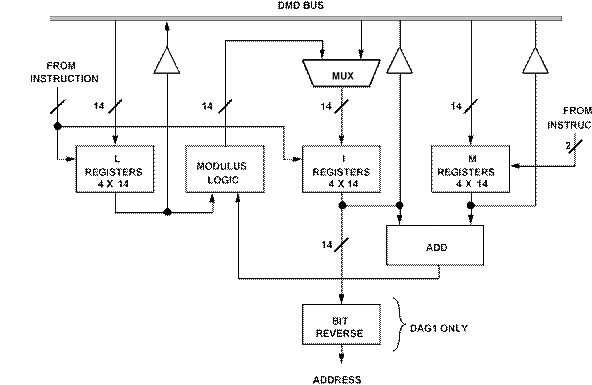
Figure 4-1, shows a block diagram of a single data address generator. There are three register files: the modify (M) register file, the index (I) register file, and the length (L) register file. Each of the register files contains four 14-bit registers that can be read from and written to via the DMD bus.
 2
2
Figure 4-1. Data Address Generator Block Diagram
The I (index) registers (I0-I3 in DAG1, I4-I7 in DAG2) contain the actual addresses used to access memory. When data is accessed in indirect mode, the address stored in the selected I register becomes the memory address. With DAG1, the output address can be bit-reversed by setting the appropriate mode bit in the mode status register (MSTAT) as discussed below or by using the ENA BIT_REV instruction. Bit-reversal facilitates FFT addressing.
The data address generators employ a post-modify scheme; after an indirect data access, the specified M (modify) register (M0-M3 in DAG1, M4-M7 in DAG2) is added to the specified I register to generate the updated I value. The choice of the I and M registers are independent within each DAG. In other words, any register in the I0-I3 set may be modified by any register in the M0-M3 set in any combination, but not by those in DAG2 (M4-M7). The modification values stored in M registers are signed numbers so that the next address can be either higher or lower.
The address generators support both linear addressing and circular addressing. The value of the L (length) register corresponding to an I register (for example, L0 would correspond to I0) determines which addressing scheme is used for that I register. For circular buffer addressing, the L register is initialized with length of the buffer. For linear addressing, the modulus logic is disabled by setting the corresponding L register to zero.
Each time an I register is selected, the corresponding L register provides the modulus logic with the length information. If the sum of the M register and the I register crosses the buffer boundary, the modified I register value is calculated by the modulus logic using the L register value.
All data address generator registers (I, M, and L registers) are loadable and readable from the lower 14 bits of the DMD bus. Since I and L register contents are considered to be unsigned, the upper 2 bits of the DMD bus are padded with zeros when reading them. M register contents are signed; when reading an M register, the upper
Уважаемый посетитель!
Чтобы распечатать файл, скачайте его (в формате Word).
Ссылка на скачивание - внизу страницы.