


B ADSP-2191 DSP I/O REGISTERS
Figure B-0.
Table B-0.
Listing B-0.
The DSP has general-purpose and dedicated registers in each of its functional blocks. The register reference information for each functional block includes bit definitions, initialization values, and (for I/O processor registers) memory mapped address. Information on each type of register is available at the following locations:
• “Core Status Registers” on page A-8
• “Computational Unit Registers” on page A-12
• “Program Sequencer Registers” on page A-16
• “Data Address Generator Registers” on page A-23
• “I/O Processor (Memory Mapped) Registers” on page B-2
When writing DSP programs, it is often necessary to set, clear, or test bits in the DSP’s registers. While these bit operations can all be done by referring to the bit’s location within a register or (for some operations) the register’s address with a hexadecimal number, it is much easier to use symbols that correspond to the bit’s or register’s name. For convenience and consistency, Analog Devices provides a header file that provides these bit and register definitions. For more information, see the “Register & Bit #Defines File (def219x.h)” on page A-26 and “Register and Bit #define File (def2191.h)” on page B-109.
Many registers have reserved bits. When writing to a register, programs may only clear (write zero to) a register’s reserved bits.
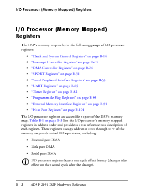
The DSP’s memory map includes the following groups of I/O processor registers:
• “Clock and System Control Registers” on page B-14
• “Interrupt Controller Registers” on page B-20
• “DMA Controller Registers” on page B-24
• “SPORT Registers” on page B-31
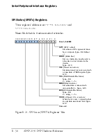
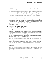
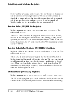
• “Serial Peripheral Interface Registers” on page B-53
• “UART Registers” on page B-65
• “Timer Registers” on page B-82
• “Programmable Flag Registers” on page B-89
• “External Memory Interface Registers” on page B-91
• “Host Port Registers” on page B-101
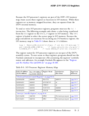
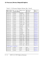
The I/O processor registers are accessible as part of the DSP’s memory map. Table B-1 on page B-3 lists the I/O processor’s memory mapped registers in address order and provides a cross reference to a description of each register. These registers occupy addresses 0x00 through 0xFF of the memory map and control I/O operations, including:
• External port DMA
• Link port DMA
• Serial port DMA
I/O processor registers have a one cycle effect latency (changes take effect on the second cycle after the change).
Because the I/O processor’s registers are part of the DSP’s I/O memory map, buses access these registers as locations in I/O memory. While these registers act as memory mapped locations, they are separate from the DSP’s internal memory.
To read or write I/O processor registers, programs must use the Io( ) instruction. The following example code shows a value being transferred from the AX0 register to the DMACW_CP register in I/O memory. The IOPG register is loaded to select the correct page in I/O memory. Because the page and address are necessary for accessing any I/O memory register, the I/O memory map in Table B-1 shows these as IOPG:Address.
iopg = Memory_DMA_Controller_Page; /* set the I/O mem page */ ax0 = WR_DMA_WORD_CONFIG; /* loads ax0 with the cfg word */ io(DMACW_CP) = ax0; /* loads DMACW_CP with the cfg word */
The register names for I/O processor registers are not part of the DSP’s assembly syntax. To ease access to these registers, programs should use the #include command to incorporate a file containing the registers’ symbolic names and addresses. An example #include file appears in the “Register and Bit #define File (def2191.h)” on page B-109.
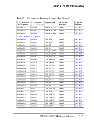
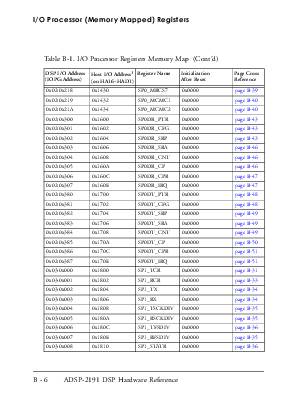
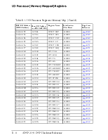
Table B-1. I/O Processor Registers Memory Map
|
DSP I/O Address (IOPG:Address) |
Host I/O Address1 (on HA16–HAD1) |
Register Name |
Initialization After Reset |
Page Cross Reference |
|
“Clock and System Control Registers” on page B-14 |
||||
|
0x00:0x200 |
0x0400 |
PLLCTL |
0x0010 |
page B-14 |
|
0x00:0x201 |
0x0402 |
LOCKCNT |
ni |
page B-17 |
|
0x00:0x202 |
0x0404 |
SWRST |
ni |
page B-17 |
|
0x00:0x203 |
0x0406 |
NXTSCR |
0x0000 |
page B-17 |
|
0x00:0x204 |
0x0408 |
SYSCR |
0x0000 |
page B-19 |
|
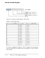
“Interrupt Controller Registers” on page B-20 |
||||
|
0x01:0x200 |
0x0C00 |
IPR0 |
Per interrupt request |
page B-20 |
|
0x01:0x201 |
0x0C02 |
IPR1 |
Per interrupt request |
page B-20 |
|
DSP I/O Address (IOPG:Address) |
Host I/O Address1 (on HA16–HAD1) |
Register Name |
Initialization After Reset |
Page Cross Reference |
|
0x01:0x202 |
0x0C04 |
IPR2 |
Per interrupt request |
page B-20 |
|
0x01:0x203 |
0x0C06 |
IPR3 |
Per interrupt request |
page B-20 |
|
0x01:0x204 |
0x0C08 |
INTRD0 |
Per interrupt request |
page B-23 |
|
0x01:0x205 |
0x0C0A |
INTRD1 |
Per interrupt request |
page B-23 |
|
0x01:0x206 |
0x0C0C |
INTRD2 |
Per interrupt request |
page B-23 |
|
0x01:0x207 |
0x0C0E |
INTRD3 |
Per interrupt request |
page B-23 |
|
0x01:0x208 |
0x0C0F |
INTRD4 |
Per interrupt request |
page B-23 |
|
0x01:0x209 |
0x0C12 |
INTRD5 |
Per interrupt request |
page B-23 |
|
0x01:0x20A |
0x0C14 |
INTRD6 |
Per interrupt request |
page B-23 |
|
0x01:0x20B |
0x0C16 |
INTRD7 |
Per interrupt request |
page B-23 |
|
0x01:0x20C |
0x0C18 |
INTRD8 |
Per interrupt request |
page B-23 |
|
0x01:0x20D |
0x0C1A |
INTRD9 |
Per interrupt request |
page B-23 |
|
0x01:0x20E |
0x0C1C |
INTRD10 |
Per interrupt request |
page B-23 |
|
0x01:0x20F |
0x0C1E |
INTRD11 |
Per interrupt request |
page B-23 |
|
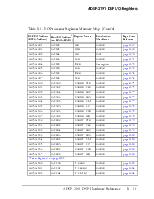
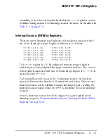
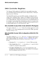
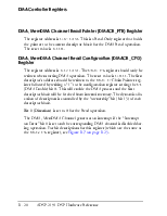
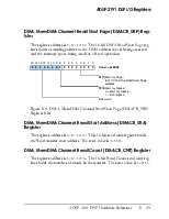
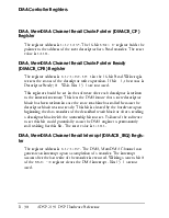
“DMA Controller Registers” on page B-24 |
||||
|
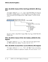
0x02:0x100 |
0x1200 |
DMACW_PTR |
0x0000 |
page B-24 |
|
0x02:0x101 |
0x1202 |
DMACW_CFG |
0x0000 |
page B-24 |
|
0x02:0x102 |
0x1204 |
DMACW_SRP |
0x0000 |
page B-26 |
|
0x02:0x103 |
0x1206 |
DMACW_SRA |
0x0000 |
page B-26 |
|
0x02:0x104 |
0x1208 |
DMACW_CNT |
0x0000 |
page B-26 |
|
0x02:0x105 |
0x120A |
DMACW_CP |
0x0000 |
page B-27 |
|
0x02:0x106 |
0x120C |
DMACW_CPR |
0x0000 |
page B-27 |
|
0x02:0x107 |
0x120E |
DMACW_IRQ |
0x0000 |
page B-27 |
|
0x02:0x180 |
0x1300 |
DMACR_PTR |
0x0000 |
page B-28 |
|
0x02:0x181 |
0x1302 |
DMACR_CFG |
0x0000 |
page B-28 |
|
0x02:0x182 |
0x1304 |
DMACR_SRP |
0x0000 |
page B-29 |
|
0x02:0x183 |
0x1306 |
DMACR_SRA |
0x0000 |
page B-29 |
|
0x02:0x184 |
0x1308 |
DMACR_CNT |
0x0000 |
page B-29 |
|
DSP I/O Address (IOPG:Address) |
Host I/O Address1 (on HA16–HAD1) |
Register Name |
Initialization After Reset |
Page Cross Reference |
|
0x02:0x185 |
0x130A |
DMACR_CP |
0x0000 |
page B-30 |
|
0x02:0x186 |
0x130C |
DMACR_CPR |
0x0000 |
page B-30 |
|
0x02:0x00187 |
0x130E |
DMACR_IRQ |
0x0000 |
page B-30 |
|
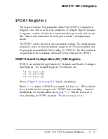
“SPORT Registers” on page B-31 |
||||
|
0x02:0x200 |
0x1400 |
SP0_TCR |
0x0000 |
page B-31 |
|
0x02:0x201 |
0x1402 |
SP0_RCR |
0x0000 |
page B-33 |
|
0x02:0x202 |
0x1404 |
SP0_TX |
0x0000 |
page B-34 |
|
0x02:0x203 |
0x1406 |
SP0_RX |
0x0000 |
page B-34 |
|
0x02:0x204 |
0x1408 |
SP0_TSCKDIV |
0x0000 |
page B-35 |
|
0x02:0x205 |
0x140A |
SP0_RSCKDIV |
0x0000 |
page B-35 |
|
0x02:0x206 |
0x140C |
SP0_TFSDIV |
0x0000 |
page B-36 |
|
0x02:0x207 |
0x140E |
SP0_RFSDIV |
0x0000 |
page B-35 |
|
0x02:0x208 |
0x1410 |
SP0_STATR |
0x0000 |
page B-36 |
|
0x02:0x209 |
0x1412 |
SP0_MTCS0 |
0x0000 |
page B-38 |
|
0x02:0x20A |
0x1414 |
SP0_MTCS1 |
0x0000 |
page B-38 |
|
0x02:0x20B |
0x1416 |
SP0_MTCS2 |
0x0000 |
page B-38 |
|
0x02:0x20C |
0x1418 |
SP0_MTCS3 |
0x0000 |
page B-38 |
|
0x02:0x20D |
0x141A |
SP0_MTCS4 |
0x0000 |
page B-38 |
|
0x02:0x20E |
0x141C |
SP0_MTCS5 |
0x0000 |
page B-38 |
|
0x02:0x20F |
0x141E |
SP0_MTCS6 |
0x0000 |
page B-38 |
|
0x02:0x210 |
0x1420 |
SP0_MTCS7 |
0x0000 |
page B-38 |
|
0x02:0x211 |
0x1422 |
SP0_MRCS0 |
0x0000 |
page B-39 |
|
0x02:0x212 |
0x1424 |
SP0_MRCS1 |
0x0000 |
page B-39 |
|
0x02:0x213 |
0x1426 |
SP0_MRCS2 |
0x0000 |
page B-39 |
|
0x02:0x214 |
0x1428 |
SP0_MRCS3 |
0x0000 |
page B-39 |
|
0x02:0x215 |
0x142A |
SP0_MRCS4 |
0x0000 |
page B-39 |
|
0x02:0x216 |
0x142C |
SP0_MRCS5 |
0x0000 |
page B-39 |
|
0x02:0x217 |
0x142E |
SP0_MRCS6 |
0x0000 |
page B-39 |
|
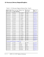
DSP I/O Address (IOPG:Address) |
Host I/O Address1 (on HA16–HAD1) |
Register Name |
Initialization After Reset |
Page Cross Reference |
|
0x02:0x218 |
0x1430 |
SP0_MRCS7 |
0x0000 |
page B-39 |
|
0x02:0x219 |
0x1432 |
SP0_MCMC1 |
0x0000 |
page B-40 |
|
0x02:0x21A |
0x1434 |
SP0_MCMC2 |
0x0000 |
page B-40 |
|
0x02:0x300 |
0x1600 |
SP0DR_PTR |
0x0000 |
page B-43 |
|
0x02:0x301 |
0x1602 |
SP0DR_CFG |
0x0000 |
page B-43 |
|
0x02:0x302 |
0x1604 |
SP0DR_SRP |
0x0000 |
page B-43 |
|
0x02:0x303 |
0x1606 |
SP0DR_SRA |
0x0000 |
page B-46 |
|
0x02:0x304 |
0x1608 |
SP0DR_CNT |
0x0000 |
page B-46 |
|
0x02:0x305 |
0x160A |
SP0DR_CP |
0x0000 |
page B-46 |
|
0x02:0x306 |
0x160C |
SP0DR_CPR |
0x0000 |
page B-47 |
|
0x02:0x307 |
0x160E |
SP0DR_IRQ |
0x0000 |
page B-47 |
|
0x02:0x380 |
0x1700 |
SP0DT_PTR |
0x0000 |
page B-48 |
|
0x02:0x381 |
0x1702 |
SP0DT_CFG |
0x0000 |
page B-48 |
|
0x02:0x382 |
0x1704 |
SP0DT_SRP |
0x0000 |
page B-49 |
|
0x02:0x383 |
0x1706 |
SP0DT_SRA |
0x0000 |
page B-49 |
|
0x02:0x384 |
0x1708 |
SP0DT_CNT |
0x0000 |
page B-49 |
|
0x02:0x385 |
0x170A |
SP0DT_CP |
0x0000 |
page B-50 |
|
0x02:0x386 |
0x170C |
SP0DT_CPR |
0x0000 |
page B-51 |
|
0x02:0x387 |
0x170E |
SP0DT_IRQ |
0x0000 |
page B-51 |
|
0x03:0x000 |
0x1800 |
SP1_TCR |
0x0000 |
page B-31 |
|
0x03:0x001 |
0x1802 |
SP1_RCR |
0x0000 |
page B-33 |
|
0x03:0x002 |
0x1804 |
SP1_TX |
0x0000 |
page B-34 |
|
0x03:0x003 |
0x1806 |
SP1_RX |
0x0000 |
page B-34 |
|
0x03:0x004 |
0x1808 |
SP1_TSCKDIV |
0x0000 |
page B-35 |
|
0x03:0x005 |
0x180A |
SP1_RSCKDIV |
0x0000 |
page B-35 |
|
0x03:0x006 |
0x180C |
SP1_TFSDIV |
0x0000 |
page B-36 |
|
0x03:0x007 |
0x180E |
SP1_RFSDIV |
0x0000 |
page B-35 |
|
0x03:0x008 |
0x1810 |
SP1_STATR |
0x0000 |
page B-36 |
|
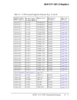
DSP I/O Address (IOPG:Address) |
Host I/O Address1 (on HA16–HAD1) |
Register Name |
Initialization After Reset |
Page Cross Reference |
|
0x03:0x009 |
0x1812 |
SP1_MTCS0 |
0x0000 |
page B-38 |
|
0x03:0x00A |
0x1814 |
SP1_MTCS1 |
0x0000 |
page B-38 |
|
0x03:0x00B |
0x1816 |
SP1_MTCS2 |
0x0000 |
page B-38 |
|
0x03:0x00C |
0x1818 |
SP1_MTCS3 |
0x0000 |
page B-38 |
|
0x03:0x00D |
0x181A |
SP1_MTCS4 |
0x0000 |
page B-38 |
|
0x03:0x00E |
0x181C |
SP1_MTCS5 |
0x0000 |
page B-38 |
|
0x03:0x00F |
0x181E |
SP1_MTCS6 |
0x0000 |
page B-38 |
|
0x03:0x010 |
0x1820 |
SP1_MTCS7 |
0x0000 |
page B-38 |
|
0x03:0x011 |
0x1822 |
SP1_MRCS0 |
0x0000 |
page B-39 |
|
0x03:0x012 |
0x1824 |
SP1_MRCS1 |
0x0000 |
page B-39 |
|
0x03:0x013 |
0x1826 |
SP1_MRCS2 |
0x0000 |
page B-39 |
|
0x03:0x014 |
0x1828 |
SP1_MRCS3 |
0x0000 |
page B-39 |
|
0x03:0x015 |
0x182A |
SP1_MRCS4 |
0x0000 |
page B-39 |
|
0x03:0x016 |
0x182C |
SP1_MRCS5 |
0x0000 |
page B-39 |
|
0x03:0x017 |
0x182E |
SP1_MRCS6 |
0x0000 |
page B-39 |
|
0x03:0x018 |
0x1830 |
SP1_MRCS7 |
0x0000 |
page B-39 |
|
0x03:0x019 |
0x1832 |
SP1_MCMC1 |
0x0000 |
page B-40 |
|
0x03:0x01A |
0x1834 |
SP1_MCMC2 |
0x0000 |
page B-40 |
|
0x03:0x100 |
0x1A00 |
SP1DR_PTR |
0x0000 |
page B-43 |
|
0x03:0x101 |
0x1A02 |
SP1DR_CFG |
0x0000 |
page B-43 |
|
0x03:0x102 |
0x1A04 |
SP1DR_SRP |
0x0000 |
page B-43 |
|
0x03:0x103 |
0x1A06 |
SP1DR_SRA |
0x0000 |
page B-46 |
|
0x03:0x104 |
0x1A08 |
SP1DR_CNT |
0x0000 |
page B-46 |
|
0x03:0x105 |
0x1A0A |
SP1DR_CP |
0x0000 |
page B-46 |
|
0x03:0x106 |
0x1A0C |
SP1DR_CPR |
0x0000 |
page B-47 |
|
0x03:0x107 |
0x1A0E |
SP1DR_IRQ |
0x0000 |
page B-47 |
|
0x03:0x180 |
0x1A10 |
SP1DT_PTR |
0x0000 |
page B-48 |
|
0x03:0x181 |
0x1A12 |
SP1DT_CFG |
0x0000 |
page B-48 |
|
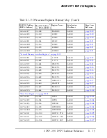
DSP I/O Address (IOPG:Address) |
Host I/O Address1 (on HA16–HAD1) |
Register Name |
Initialization After Reset |
Page Cross Reference |
|
0x03:0x182 |
0x1A14 |
SP1DT_SRP |
0x0000 |
page B-49 |
|
0x03:0x183 |
0x1A16 |
SP1DT_SRA |
0x0000 |
page B-49 |
|
0x03:0x184 |
0x1A18 |
SP1DT_CNT |
0x0000 |
page B-49 |
|
0x03:0x185 |
0x1A1A |
SP1DT_CP |
0x0000 |
page B-50 |
|
0x03:0x186 |
0x1A1C |
SP1DT_CPR |
0x0000 |
page B-51 |
|
0x03:0x187 |
0x1A1E |
SP1DT_IRQ |
0x0000 |
page B-51 |
|
0x03:0x200 |
0x1C00 |
SP2_TCR |
0x0000 |
page B-31 |
|
0x03:0x201 |
0x1C02 |
SP2_RCR |
0x0000 |
page B-33 |
|
0x03:0x202 |
0x1C04 |
SP2_TX |
0x0000 |
page B-34 |
|
0x03:0x203 |
0x1C06 |
SP2_RX |
0x0000 |
page B-34 |
|
0x03:0x204 |
0x1C08 |
SP2_TSCKDIV |
0x0000 |
page B-35 |
|
0x03:0x205 |
0x1C0A |
SP2_RSCKDIV |
0x0000 |
page B-35 |
|
0x03:0x206 |
0x1C0C |
SP2_TFSDIV |
0x0000 |
page B-36 |
|
0x03:0x207 |
0x1C0E |
SP2_RFSDIV |
0x0000 |
page B-35 |
|
0x03:0x208 |
0x1C10 |
SP2_STATR |
0x0000 |
page B-36 |
|
0x03:0x209 |
0x1C12 |
SP2_MTCS0 |
0x0000 |
page B-38 |
|
0x03:0x20A |
0x1C14 |
SP2_MTCS1 |
0x0000 |
page B-38 |
|
0x03:0x20B |
0x1C16 |
SP2_MTCS2 |
0x0000 |
page B-38 |
|
0x03:0x20C |
0x1C18 |
SP2_MTCS3 |
0x0000 |
page B-38 |
|
0x03:0x20D |
0x1C1A |
SP2_MTCS4 |
0x0000 |
page B-38 |
|
0x03:0x20E |
0x1C1C |
SP2_MTCS5 |
0x0000 |
page B-38 |
|
0x03:0x20F |
0x1C1E |
SP2_MTCS6 |
0x0000 |
page B-38 |
|
0x03:0x210 |
0x1C20 |
SP2_MTCS7 |
0x0000 |
page B-38 |
|
0x03:0x211 |
0x1C22 |
SP2_MRCS0 |
0x0000 |
page B-39 |
|
0x03:0x212 |
0x1C24 |
SP2_MRCS1 |
0x0000 |
page B-39 |
|
0x03:0x213 |
0x1C26 |
SP2_MRCS2 |
0x0000 |
page B-39 |
|
0x03:0x214 |
0x1C28 |
SP2_MRCS3 |
0x0000 |
page B-39 |
|
0x03:0x215 |
0x1C2A |
SP2_MRCS4 |
0x0000 |
page B-39 |
|
DSP I/O Address (IOPG:Address) |
Host I/O Address1 (on HA16–HAD1) |
Register Name |
Initialization After Reset |
Page Cross Reference |
|
0x03:0x216 |
0x1C2C |
SP2_MRCS5 |
0x0000 |
page B-39 |
|
0x03:0x217 |
0x1C2E |
SP2_MRCS6 |
0x0000 |
page B-39 |
|
0x03:0x218 |
0x1C30 |
SP2_MRCS7 |
0x0000 |
page B-39 |
|
0x03:0x219 |
0x1C32 |
SP2_MCMC1 |
0x0000 |
page B-40 |
|
0x03:0x21A |
0x1C34 |
SP2_MCMC2 |
0x0000 |
page B-40 |
|
0x03:0x300 |
0x1E00 |
SP2DR_PTR |
0x0000 |
page B-43 |
|
0x03:0x301 |
0x1E02 |
SP2DR_CFG |
0x0000 |
page B-43 |
|
0x03:0x302 |
0x1E04 |
SP2DR_SRP |
0x0000 |
page B-43 |
|
0x03:0x303 |
0x1E06 |
SP2DR_SRA |
0x0000 |
page B-46 |
|
0x03:0x304 |
0x1E08 |
SP2DR_CNT |
0x0000 |
page B-46 |
|
0x03:0x305 |
0x1E0A |
SP2DR_CP |
0x0000 |
page B-46 |
|
0x03:0x306 |
0x1E0C |
SP2DR_CPR |
0x0000 |
page B-47 |
|
0x03:0x307 |
0x1E0E |
SP2DR_IRQ |
0x0000 |
page B-47 |
|
0x03:0x380 |
0x1E10 |
SP2DT_PTR |
0x0000 |
page B-48 |
|
0x03:0x381 |
0x1E12 |
SP2DT_CFG |
0x0000 |
page B-48 |
|
0x03:0x382 |
0x1E14 |
SP2DT_SRP |
0x0000 |
page B-49 |
|
0x03:0x383 |
0x1E16 |
SP2DT_SRA |
0x0000 |
page B-49 |
|
0x03:0x384 |
0x1E18 |
SP2DT_CNT |
0x0000 |
page B-49 |
|
0x03:0x385 |
0x1E1A |
SP2DT_CP |
0x0000 |
page B-50 |
|
0x03:0x386 |
0x1E1C |
SP2DT_CPR |
0x0000 |
page B-51 |
|
0x03:0x387 |
0x1E1E |
SP2DT_IRQ |
0x0000 |
page B-51 |
|
“Serial Peripheral Interface Registers” on page B-53 |
||||
|
0x04:0x000 |
0x2000 |
SPICTL0 |
0x0400 |
page B-53 |
|
0x04:0x001 |
0x2002 |
SPIFLG0 |
0xFF00 |
page B-56 |
|
0x04:0x002 |
0x20024 |
SPIST0 |
0x01 |
page B-58 |
|
0x04:0x003 |
0x2006 |
TDBR0 |
0x0000 |
page B-59 |
|
0x04:0x004 |
0x2008 |
RDBR0 |
0x0000 |
page B-60 |
|
0x04:0x005 |
0x200A |
SPIBAUD0 |
0x0000 |
page B-60 |
|
DSP I/O Address (IOPG:Address) |
Host I/O Address1 (on HA16–HAD1) |
Register Name |
Initialization After Reset |
Page Cross Reference |
|
0x04:0x006 |
0x200C |
RDBRS0 |
0x0000 |
page B-60 |
|
0x04:0x100 |
0x2200 |
SPI0D_PTR |
0x0000 |
page B-61 |
|
0x04:0x101 |
0x2202 |
SPI0D_CFG |
0x0000 |
page B-61 |
|
0x04:0x102 |
0x2204 |
SPI0D_SRP |
0x0000 |
page B-63 |
|
0x04:0x103 |
0x2206 |
SPI0D_SRA |
0x0000 |
page B-63 |
|
0x04:0x104 |
0x2208 |
SPI0D_CNT |
0x0000 |
page B-63 |
|
0x04:0x105 |
0x220A |
SPI0D_CP |
0x0000 |
page B-63 |
|
0x04:0x106 |
0x220C |
SPI0D_CPR |
0x0000 |
page B-64 |
|
0x04:0x107 |
0x220E |
SPI0D_IRQ |
0x0000 |
page B-64 |
|
0x04:0x200 |
0x2400 |
SPICTL1 |
0x0400 |
page B-53 |
|
0x04:0x201 |
0x2402 |
SPIFLG1 |
0xFF00 |
page B-56 |
|
0x04:0x202 |
0x2404 |
SPIST1 |
0x01 |
page B-58 |
|
0x04:0x203 |
0x2406 |
TDBR1 |
0x0000 |
page B-59 |
|
0x04:0x204 |
0x2408 |
RDBR1 |
0x0000 |
page B-60 |
|
0x04:0x205 |
0x240A |
SPIBAUD1 |
0x0000 |
page B-60 |
|
0x04:0x206 |
0x240C |
RDBRS1 |
0x0000 |
page B-60 |
|
0x04:0x300 |
0x2600 |
SPI1D_PTR |
0x0000 |
page B-61 |
|
0x04:0x301 |
0x2602 |
SPI1D_CFG |
0x0000 |
page B-61 |
|
0x04:0x302 |
0x2604 |
SPI1D_SRP |
0x0000 |
page B-63 |
|
0x04:0x303 |
0x2606 |
SPI1D_SRA |
0x0000 |
page B-63 |
|
0x04:0x304 |
0x2608 |
SPI1D_CNT |
0x0000 |
page B-63 |
|
0x04:0x305 |
0x260A |
SPI1D_CP |
0x0000 |
page B-63 |
|
0x04:0x306 |
0x260C |
SPI1D_CPR |
0x0000 |
page B-64 |
|
0x04:0x307 |
0x260E |
SPI1D_IRQ |
0x0000 |
page B-64 |
|
“UART Registers” on page B-65 |
||||
|
0x05:0x000 |
0x2800 |
THR |
0x01 |
page B-66 |
|
0x05:0x000 |
0x2800 |
RBR |
0x0000 |
page B-67 |
|
0x05:0x000 |
0x2800 |
DLL |
0x0000 |
page B-68 |
|
DSP I/O Address (IOPG:Address) |
Host I/O Address1 (on HA16–HAD1) |
Register Name |
Initialization After Reset |
Page Cross Reference |
|
0x05:0x001 |
0x2802 |
IER |
0x0000 |
page B-67 |
|
0x05:0x001 |
0x2802 |
DLH |
0x0000 |
page B-68 |
|
0x05:0x002 |
0x2804 |
IIR |
0x01 |
page B-70 |
|
0x05:0x003 |
0x2806 |
LCR |
0x0000 |
page B-71 |
|
0x05:0x004 |
0x2808 |
MCR |
See register |
page B-72 |
|
0x05:0x005 |
0x280A |
LSR |
0x0060 |
page B-73 |
|
0x05:0x006 |
0x280C |
MSR |
0x0000 |
page B-74 |
|
0x05:0x007 |
0x280E |
SCR |
0x0000 |
page B-74 |
|
0x05:0x100 |
0x2A00 |
UARDR_PTR |
0x0000 |
page B-75 |
|
0x05:0x101 |
0x2A02 |
UARDR_CFG |
0x0000 |
page B-75 |
|
0x05:0x102 |
0x2A04 |
UARDR_SRP |
0x0000 |
page B-77 |
|
0x05:0x103 |
0x2A06 |
UARDR_SRA |
0x0000 |
page B-77 |
|
0x05:0x104 |
0x2A08 |
UARDR_CNT |
0x0000 |
page B-77 |
|
0x05:0x105 |
0x2A0A |
UARDR_CP |
0x0000 |
page B-78 |
|
0x05:0x106 |
0x2A0C |
UARDR_CPR |
0x0000 |
page B-78 |
|
0x05:0x107 |
0x2A0E |
UARDR_IRQ |
0x0000 |
page B-78 |
|
0x05:0x180 |
0x2B00 |
UARDT_PTR |
0x0000 |
page B-79 |
|
0x05:0x181 |
0x2B02 |
UARDT_CFG |
0x0000 |
page B-79 |
|
0x05:0x182 |
0x2B04 |
UARDT_SRP |
0x0000 |
page B-79 |
|
0x05:0x183 |
0x2B06 |
UARDT_SRA |
0x0000 |
page B-80 |
|
0x05:0x184 |
0x2B08 |
UARDT_CNT |
0x0000 |
page B-80 |
|
0x05:0x185 |
0x2B0A |
UARDT_CP |
0x0000 |
page B-80 |
|
0x05:0x186 |
0x2B0C |
UARDT_CPR |
0x0000 |
page B-80 |
|
0x05:0x187 |
0x2B0E |
UARDT_IRQ |
0x0000 |
page B-80 |
|
“Timer Registers” on page B-82 |
||||
|
0x05:0x200 |
0x2C00 |
T_GSR0 |
0x0000 |
page B-82 |
|
0x05:0x201 |
0x2C02 |
T_CFGR0 |
0x0000 |
page B-84 |
|
0x05:0x202 |
0x2C04 |
T_CNTL0 |
0x0000 |
page B-84 |
|
DSP I/O Address (IOPG:Address) |
Host I/O Address1 (on HA16–HAD1) |
Register Name |
Initialization After Reset |
Page Cross Reference |
|
0x05:0x203 |
0x2C06 |
T_CNTH0 |
0x0000 |
page B-84 |
|
0x05:0x204 |
0x2C08 |
T_PRDL0 |
0x0000 |
page B-86 |
|
0x05:0x205 |
0x2C0A |
T_PRDH0 |
0x0000 |
page B-86 |
|
0x05:0x206 |
0x2C0C |
T_WLR0 |
0x0000 |
page B-87 |
|
0x05:0x207 |
0x2C0E |
T_WHR0 |
0x0000 |
page B-87 |
|
0x05:0x208 |
0x2C10 |
T_GSR1 |
0x0000 |
page B-82 |
|
0x05:0x209 |
0x2C12 |
T_CFGR1 |
0x0000 |
page B-84 |
|
0x05:0x20A |
0x2C14 |
T_CNTL1 |
0x0000 |
page B-84 |
|
0x05:0x20B |
0x2C16 |
T_CNTH1 |
0x0000 |
page B-84 |
|
0x05:0x20C |
0x2C18 |
T_PRDL1 |
0x0000 |
page B-86 |
|
0x05:0x20D |
0x2C1A |
T_PRDH1 |
0x0000 |
page B-86 |
|
0x05:0x20E |
0x2C1C |
T_WLR1 |
0x0000 |
page B-87 |
|
0x05:0x20F |
0x2C1E |
T_WHR1 |
0x0000 |
page B-87 |
|
0x05:0x210 |
0x2C20 |
T_GSR2 |
0x0000 |
page B-82 |
|
0x05:0x211 |
0x2C22 |
T_CFGR2 |
0x0000 |
page B-84 |
|
0x05:0x212 |
0x2C24 |
T_CNTL2 |
0x0000 |
page B-84 |
|
0x05:0x213 |
0x2C26 |
T_CNTH2 |
0x0000 |
page B-84 |
|
0x05:0x214 |
0x2C28 |
T_PRDL2 |
0x0000 |
page B-86 |
|
0x05:0x215 |
0x2C2A |
T_PRDH2 |
0x0000 |
page B-86 |
|
0x05:0x216 |
0x2C2C |
T_WLR2 |
0x0000 |
page B-87 |
|
0x05:0x217 |
0x2C2E |
T_WHR2 |
0x0000 |
page B-87 |
|
“Programmable Flag Registers” on page B-89 |
||||
|
0x06:0x000 |
0x3000 |
DIR |
0x0000 |
page B-89 |
|
0x06:0x002 |
0x3004 |
FLAGC |
Input |
page B-89 |
|
0x06:0x003 |
0x3006 |
FLAGS |
Input |
page B-89 |
|
0x06:0x004 |
0x3008 |
MASKAC |
0x0000 |
page B-89 |
|
0x06:0x005 |
0x300A |
MASKAS |
0x0000 |
page B-89 |
|
0x06:0x006 |
0x300C |
MASKBC |
0x0000 |
page B-89 |
|
DSP I/O Address (IOPG:Address) |
Host I/O Address1 (on HA16–HAD1) |
Register Name |
Initialization After Reset |
Page Cross Reference |
|
0x06:0x007 |
0x300E |
MASKBS |
0x0000 |
page B-89 |
|
0x06:0x008 |
0x3010 |
FSPRC |
0x0000 |
page B-90 |
|
0x06:0x009 |
0x3012 |
FSPRS |
0x0000 |
page B-90 |
|
0x06:0x00A |
0x3014 |
FSSRC |
0x0000 |
page B-91 |
|
0x06:0x00B |
0x3016 |
FSSRS |
0x0000 |
page B-91 |
|
0x06:0x00C |
0x3018 |
FSBERC |
0x0000 |
page B-91 |
|
0x06:0x00D |
0x301A |
FSBERS |
0x0000 |
page B-91 |
|
“External Memory Interface Registers” on page B-91 |
||||
|
0x00:0x080 |
0x0100 |
E_STAT |
0x0300 |
page B-92 |
|
0x06:0x201 |
0x3402 |
E_CTL |
0x0300 |
page B-93 |
|
0x06:0x202 |
0x3404 |
BMSCTL |
0x0000 |
page B-94 |
|
0x06:0x203 |
0x3406 |
MS0CTL |
0x0000 |
page B-96 |
|
0x06:0x204 |
0x3408 |
MS1CTL |
0x0000 |
page B-96 |
|
0x06:0x205 |
0x340A |
MS2CTL |
0x0000 |
page B-96 |
|
0x06:0x206 |
0x340C |
MS3CTL |
0x0000 |
page B-96 |
|
0x06:0x207 |
0x340E |
IOMSCTL |
0x0000 |
page B-97 |
|
0x06:0x208 |
0x3410 |
EMISTAT |
0x0000 |
page B-97 |
|
0x06:0x209 |
0x3412 |
MSPG10 |
0x0000 |
page B-100 |
|
0x06:0x20A |
0x3414 |
MSPG32 |
0x0000 |
page B-100 |
|
“Host Port Registers” on page B-101 |
||||
|
0x07:0x001 |
0x3802 |
HPCR |
0x0000 |
page B-101 |
|
0x07:0x002 |
0x3804 |
HPPR |
0x0000 |
page B-104 |
|
0x07:0x003 |
0x3806 |
HPDER |
0x0000 |
page B-104 |
|
0x07:0x0FC |
0x39F8 |
HPSMPHA |
0x0000 |
page B-104 |
|
0x07:0x0FD |
0x39FA |
HPSMPHB |
0x0000 |
page B-104 |
|
0x07:0x100 |
0x3A00 |
HOSTD_PTR |
0x0000 |
page B-105 |
|
0x07:0x101 |
0x3A02 |
HOSTD_CFG |
0x0000 |
page B-105 |
|
0x07:0x102 |
0x3A04 |
HOSTD_SRP |
0x0000 |
page B-107 |
|
DSP I/O Address (IOPG:Address) |
Host I/O Address1 (on HA16–HAD1) |
Register Name |
Initialization After Reset |
Page Cross Reference |
|
0x07:0x103 |
0x3A06 |
HOSTD_SRA |
0x0000 |
page B-107 |
|
0x07:0x104 |
0x3A08 |
HOSTD_CNT |
0x0000 |
page B-107 |
|
0x07:0x105 |
0x3A0A |
HOSTD_CP |
0x0000 |
page B-107 |
|
0x07:0x106 |
0x3A0C |
HOSTD_CPR |
0x0000 |
page B-108 |
|
0x07:0x107 |
0x3A0E |
HOSTD_IRQ |
0x0000 |
page B-108 |
1 HAD0 usage depends on Host port configuration.
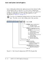
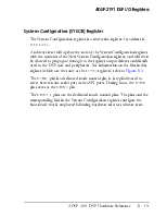
Clock and System Control group of I/P registers include:
• “PLL Control (PLLCTL) Register” on page B-14
• “PLL Lock Counter (LOCKCNT) Register” on page B-17
• “Software Reset (SWRST) Register” on page B-17
• “Next System Configuration (NXTSCR) Register” on page B-17
• “System Configuration (SYSCR) Register” on page B-19
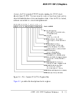
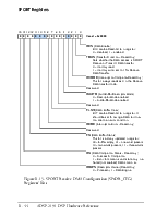
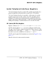
PLL Control (PLLCTL) Register
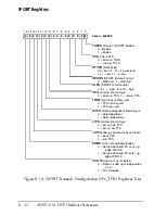
The PLL Control (PLLCTL) register lets systems select and change the DSP’s core clock (CCLK) frequency and select powerdown modes. The PLL multiplies the clock frequency of the input clock with a programmable ratio. The PLL Control register address is 0x00:0x200.
At reset, the PLL starts in BYPASS mode, running the CCLK clock directly from CLKIN. The reset must be active at least four clock cycle to allow full initialization of the synchronizer chain. After the PLL is locked, software can switch to a clock multiplier mode.
15 14 13 12 11 10 9 8 7 6 5 4 3 2 1 0
 0 0 0 0 1 0 0 0 0 Reset
= 0x0010
0 0 0 0 1 0 0 0 0 Reset
= 0x0010
DF (Divide Frequency)
00/01=No PLL, 10=CLKIN to PLL,
11=CLKIN/2 to PLL
PO (PLL Off)
0= PLL on, 1= PLL off
STOPALL (Stop All PLL Output)
0=PLL output, 1=CCLK and HCLK high
STOPCK (Stop Core Clock)
0=CCLK output, 1=CCLK high
IOSEL (Core:Peripheral Clock Ratio)
0=HCLK=CCLK, 1=HCLK=CCLK/2
PDWN (Powerdown)
0=run, 1=Powerdown all CKOUTEN (CLKOUT Enable)
0=CLKOUT=0, 1=CLKOUT=HCLK
DIV2 (Divide CLKIN /2 In Bypass Enable)
0=no divide, 1=CCLK=CLKIN/2 in Bypass
BYPASS (Bypass PLL Multiplier)
0=Multiplier mode, 1=Bypass mode
MSEL4–0 (CLKIN Multiply Ratio)
00 = 0 to 15, 01 =16 to 31,
10 = 0.5 to 15.5, 11 = 0 to 15
MSEL5 (Second Stage Multiplier Enable)
MSEL6 (Output Multiplier Enable)
Figure B-1. PLL Control (PLLCTL) Register Bits
Figure B-1 provides bit descriptions for the register.
Refer to
“Using The PLL Control (PLLCTL) Register” on page 14-35 for
more information.
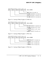
PLL Lock Counter (LOCKCNT) Register
The Lock Counter is a 10-bit register. The register address is 0x00:0x201.
The process of changing the multiplication factor of the PLL takes a certain number of cycles, and therefore a Lock Counter is required in order to calculate when the PLL is locked to the new ratio. The value of the Lock Counter depends on the frequency (the higher
Уважаемый посетитель!
Чтобы распечатать файл, скачайте его (в формате Word).
Ссылка на скачивание - внизу страницы.