 HFA3046, HFA3096,
HFA3127, HFA3128
July 1995 Ultra High Frequency Transistor Array
|
|
CAUTION: These devices are sensitive to electrostatic discharge. Users should follow proper IC Handling Procedures. File Number 3076.6
Copyright © Harris Corporation 1995
|
Absolute Maximum Ratings |
Thermal Information |
|
Collector to Emitter Voltage (Open Base). . . . . . . . . . . . . . . . . .8.0V Collector to Base Voltage (Shorted Base) . . . . . . . . . . . . . . . 12.0V Emitter to Base Voltage (Reverse Bias). . . . . . . . . . . . . . . . . . 5.5V Collector Current . . . . . . . . . . . . . . . . . . . . . . . . . . . . . . . . . 15.5mA Storage Temperature Range . . . . . . . . . . . . . . . . . -65oC to +150oC Operating Temperature Range. . . . . . . . . . . . . . . . -55oC to +125oC Junction Temperature (Die) . . . . . . . . . . . . . . . . . . . . . . . . . +175oC Junction Temperature (Plastic Package) . . . . . . . . . . . . . . . +150oC Lead Temperature (Soldering 10s) (Lead Tips Only. . . . . . . +300oC |
Thermal Resistance θJA Plastic 14 Lead SOIC Package . . . . . . . . . . . . . . . . . . 120oC/W Plastic 16 Lead SOIC Package . . . . . . . . . . . . . . . . . . 115oC/W Maximum Package Power Dissipation at +75oC Plastic 14 Lead SOIC Package . . . . . . . . . . . . . . . . . . . . . . 0.63W Plastic 16 Lead SOIC Package . . . . . . . . . . . . . . . . . . . . . . 0.66W Any One Transistor . . . . . . . . . . . . . . . . . . . . . . . . . . . . . . . 0.15W Derating Factor Above +75oC Plastic 14 Lead SOIC Package . . . . . . . . . . . . . . . . . . .8.4mW/oC Plastic 16 Lead SOIC Package . . . . . . . . . . . . . . . . . . .8.7mW/oC |
CAUTION: Stresses above those listed in “Absolute Maximum Ratings” may cause permanent damage to the device. This is a stress only rating and operation of the device at these or any other conditions above those indicated in the operational sections of this specification is not implied.
![]()
Static NPN Characteristics at TA = +25oC
|
PARAMETERS |
TEST CONDITIONS |
DIE |
SOIC |
UNITS |
||||
|
MIN |
TYP |
MAX |
MIN |
TYP |
MAX |
|||
|
Collector-to-Base Breakdown Voltage, V(BR)CBO |
IC = 100µA, IE = 0 |
12 |
18 |
- |
12 |
18 |
- |
V |
|
Collector-to-Emitter Breakdown Voltage, V(BR)CEO |
IC = 100µA, IB = 0 |
8 |
12 |
- |
8 |
12 |
- |
V |
|
Collector-to-Emitter Breakdown Voltage, V(BR)CES |
IC = 100µA, Base Shorted to Emitter |
10 |
20 |
- |
10 |
20 |
- |
V |
|
Emitter-to-Base Breakdown Voltage, V(BR)EBO |
IE = 10µA, IC = 0 |
5.5 |
6 |
- |
5.5 |
6 |
- |
V |
|
Collector-Cutoff-Current, ICEO |
VCE = 6V, IB = 0 |
- |
2 |
100 |
- |
2 |
100 |
nA |
|
Collector-Cutoff-Current, ICBO |
VCB = 8V, IE = 0 |
- |
0.1 |
10 |
- |
0.1 |
10 |
nA |
|
Collector-to-Emitter Saturation Voltage, VCE(SAT) |
IC = 10mA, IB = 1mA |
- |
0.3 |
0.5 |
- |
0.3 |
0.5 |
V |
|
Base-to-Emitter Voltage, VBE |
IC = 10mA |
- |
0.85 |
0.95 |
- |
0.85 |
0.95 |
V |
|
DC Forward-Current Transfer Ratio, hFE |
IC = 10mA VCE = 2V |
40 |
70 |
- |
40 |
70 |
- |
|
|
Early Voltage, VA |
IC = 1mA, VCE = 3.5V |
20 |
50 |
- |
20 |
50 |
- |
V |
|
Base-to-Emitter Voltage Drift |
IC = 10mA |
- |
-1.5 |
- |
- |
-1.5 |
- |
mV/oC |
|
Collector-to-Collector Leakage |
- |
1 |
- |
- |
1 |
- |
pA |
|
Dynamic NPN Characteristics at TA = +25oC
|
PARAMETERS |
TEST CONDITIONS |
DIE |
SOIC |
UNITS |
||||
|
MIN |
TYP |
MAX |
MIN |
TYP |
MAX |
|||
|
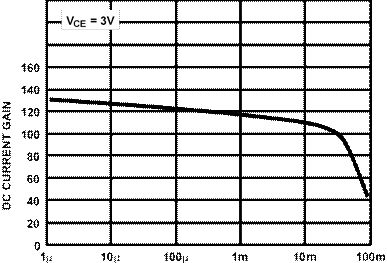
Noise Figure |
f = 1.0GHz, VCE = 5V, IC = 5mA, ZS = 50Ω |
- |
3.5 |
- |
- |
3.5 |
- |
dB |
|
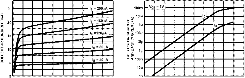
fT Current Gain-Bandwidth Product |
IC = 1mA, VCE = 5V |
- |
5.5 |
- |
- |
5.5 |
- |
GHz |
|
IC = 10mA, VCE = 5V |
- |
8 |
- |
- |
8 |
- |
GHz |
|
|
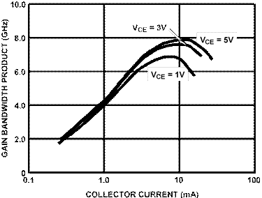
Power Gain-Bandwidth Product, fMAX |
IC = 10mA, VCE = 5V |
- |
6 |
- |
- |
2.5 |
- |
GHz |
|
Base-to-Emitter Capacitance |
VBE = -3V |
- |
200 |
- |
- |
500 |
- |
fF |
|
Collector-to-Base Capacitance |
VCB = 3V |
- |
200 |
- |
- |
500 |
- |
fF |
Static PNP Characteristics at TA = +25oC
|
PARAMETERS |
TEST CONDITIONS |
DIE |
SOIC |
UNITS |
||||
|
MIN |
TYP |
MAX |
MIN |
TYP |
MAX |
|||
|
Collector-to-Base Breakdown Voltage, V(BR)CBO |
IC = -100µA, IE = 0 |
10 |
15 |
- |
10 |
15 |
- |
V |
|
Collector-to-Emitter Breakdown Voltage, V(BR)CEO |
IC = -100µA, IB = 0 |
8 |
15 |
- |
8 |
15 |
- |
V |
|
Collector-to-Emitter Breakdown Voltage, V(BR)CES |
IC = -100µA, Base Shorted to Emitter |
10 |
15 |
- |
10 |
15 |
- |
V |
|
Emitter-to-Base Breakdown Voltage, V(BR)EBO |
IE = -10µA, IC = 0 |
4.5 |
5 |
- |
4.5 |
5 |
- |
V |
|
Collector-Cutoff-Current, ICEO |
VCE = -6V, IB = 0 |
- |
2 |
100 |
- |
2 |
100 |
nA |
|
Collector-Cutoff-Current, ICBO |
VCB = -8V, IE = 0 |
- |
0.1 |
10 |
- |
0.1 |
10 |
nA |
|
Collector-to-Emitter Saturation Voltage, VCE(SAT) |
IC = -10mA, IB = -1mA |
- |
0.3 |
0.5 |
- |
0.3 |
0.5 |
V |
|
Base-to-Emitter Voltage, VBE |
IC = -10mA |
- |
0.85 |
0.95 |
- |
0.85 |
0.95 |
V |
|
DC Forward-Current Transfer Ratio, hFE |
IC = -10mA, VCE = -2V |
25 |
40 |
- |
25 |
40 |
- |
|
|
Early Voltage, VA |
IC = -1mA, VCE = -3.5V |
10 |
25 |
- |
10 |
25 |
- |
V |
|
Base-to-Emitter Voltage Drift |
IC = -10mA |
- |
-1.5 |
- |
- |
-1.5 |
- |
mV/oC |
|
Collector-to-Collector Leakage |
- |
1 |
- |
- |
1 |
- |
pA |
|
Dynamic PNP Characteristics at TA = +25oC
|
PARAMETERS |
TEST CONDITIONS |
DIE |
SOIC |
UNITS |
||||
|
MIN |
TYP |
MAX |
MIN |
TYP |
MAX |
|||
|
Noise Figure |
f = 1.0GHz, VCE = -5V, IC = -5mA, ZS = 50Ω |
- |
3.5 |
- |
- |
3.5 |
- |
dB |
|
fT Current Gain-Bandwidth Product |
IC = -1mA, VCE = -5V |
- |
2 |
- |
- |
2 |
- |
GHz |
|
IC = -10mA, VCE = -5V |
- |
5.5 |
- |
- |
5.5 |
- |
GHz |
|
|
Power Gain-Bandwidth Product |
IC = -10mA, VCE = -5V |
- |
3 |
- |
- |
2 |
- |
GHz |
|
Base-to-Emitter Capacitance |
VBE = 3V |
- |
200 |
- |
- |
500 |
- |
fF |
|
Collector-to-Base Capacitance |
VCB = -3V |
- |
300 |
- |
- |
600 |
- |
fF |
Differential Pair Matching Characteristics for the HFA3046
|
PARAMETERS |
TEST CONDITIONS |
DIE |
SOIC |
UNITS |
||||
|
MIN |
TYP |
MAX |
MIN |
TYP |
MAX |
|||
|
Input Offset Voltage |
IC = 10mA, VCE = 5V |
- |
1.5 |
5.0 |
- |
1.5 |
5.0 |
mV |
|
Input Offset Current |
IC = 10mA, VCE = 5V |
- |
5 |
25 |
- |
5 |
25 |
µA |
|
Input Offset Voltage TC |
IC = 10mA, VCE = 5V |
- |
0.5 |
- |
- |
0.5 |
- |
µV/oC |
S-Parameter and PSPICE model data is available from Harris Sales Offices.
Common Emitter S-Parameters of NPN 3µm x 50µm Transistor
|
FREQ. (Hz) |
|S11| |
PHASE(S11) |
|S12| |
PHASE(S12) |
|S21| |
PHASE(S21) |
|S22| |
PHASE(S22) |
|
VCE = 5V and IC = 5mA |
||||||||
|
1.0E+08 |
0.83 |
-11.78 |
1.41E-02 |
78.88 |
11.07 |
168.57 |
0.97 |
-11.05 |
|
2.0E+08 |
0.79 |
-22.82 |
2.69E-02 |
68.63 |
10.51 |
157.89 |
0.93 |
-21.35 |
|
3.0E+08 |
0.73 |
-32.64 |
3.75E-02 |
59.58 |
9.75 |
148.44 |
0.86 |
-30.44 |
|
4.0E+08 |
0.67 |
-41.08 |
4.57E-02 |
51.90 |
8.91 |
140.36 |
0.79 |
-38.16 |
|
5.0E+08 |
0.61 |
-48.23 |
5.19E-02 |
45.50 |
8.10 |
133.56 |
0.73 |
-44.59 |
|
6.0E+08 |
0.55 |
-54.27 |
5.65E-02 |
40.21 |
7.35 |
127.88 |
0.67 |
-49.93 |
|
7.0E+08 |
0.50 |
-59.41 |
6.00E-02 |
35.82 |
6.69 |
123.10 |
0.62 |
-54.37 |
|
8.0E+08 |
0.46 |
-63.81 |
6.27E-02 |
32.15 |
6.11 |
119.04 |
0.57 |
-58.10 |
|
9.0E+08 |
0.42 |
-67.63 |
6.47E-02 |
29.07 |
5.61 |
115.57 |
0.53 |
-61.25 |
|
1.0E+09 |
0.39 |
-70.98 |
6.63E-02 |
26.45 |
5.17 |
112.55 |
0.50 |
-63.96 |
|
1.1E+09 |
0.36 |
-73.95 |
6.75E-02 |
24.19 |
4.79 |
109.91 |
0.47 |
-66.31 |
|
1.2E+09 |
0.34 |
-76.62 |
6.85E-02 |
22.24 |
4.45 |
107.57 |
0.45 |
-68.37 |
|
1.3E+09 |
0.32 |
-79.04 |
6.93E-02 |
20.53 |
4.15 |
105.47 |
0.43 |
-70.19 |
|
1.4E+09 |
0.30 |
-81.25 |
7.00E-02 |
19.02 |
3.89 |
103.57 |
0.41 |
-71.83 |
|
1.5E+09 |
0.28 |
-83.28 |
7.05E-02 |
17.69 |
3.66 |
101.84 |
0.40 |
-73.31 |
|
1.6E+09 |
0.27 |
-85.17 |
7.10E-02 |
16.49 |
3.45 |
100.26 |
0.39 |
-74.66 |
|
1.7E+09 |
0.25 |
-86.92 |
7.13E-02 |
15.41 |
3.27 |
98.79 |
0.38 |
-75.90 |
|
1.8E+09 |
0.24 |
-88.57 |
7.17E-02 |
14.43 |
3.10 |
97.43 |
0.37 |
-77.05 |
|
1.9E+09 |
0.23 |
-90.12 |
7.19E-02 |
13.54 |
2.94 |
96.15 |
0.36 |
-78.12 |
|
2.0E+09 |
0.22 |
-91.59 |
7.21E-02 |
12.73 |
2.80 |
94.95 |
0.35 |
-79.13 |
|
2.1E+09 |
0.21 |
-92.98 |
7.23E-02 |
11.98 |
2.68 |
93.81 |
0.35 |
-80.09 |
|
2.2E+09 |
0.20 |
-94.30 |
7.25E-02 |
11.29 |
2.56 |
92.73 |
0.34 |
-80.99 |
|
2.3E+09 |
0.20 |
-95.57 |
7.27E-02 |
10.64 |
2.45 |
91.70 |
0.34 |
-81.85 |
|
2.4E+09 |
0.19 |
-96.78 |
7.28E-02 |
10.05 |
2.35 |
90.72 |
0.33 |
-82.68 |
|
2.5E+09 |
0.18 |
-97.93 |
7.29E-02 |
9.49 |
2.26 |
89.78 |
0.33 |
-83.47 |
|
2.6E+09 |
0.18 |
-99.05 |
7.30E-02 |
8.96 |
2.18 |
88.87 |
0.33 |
-84.23 |
|
2.7E+09 |
0.17 |
-100.12 |
7.31E-02 |
8.47 |
2.10 |
88.00 |
0.33 |
-84.97 |
|
2.8E+09 |
0.17 |
-101.15 |
7.31E-02 |
8.01 |
2.02 |
87.15 |
0.33 |
-85.68 |
|
2.9E+09 |
0.16 |
-102.15 |
7.32E-02 |
7.57 |
1.96 |
86.33 |
0.33 |
-86.37 |
|
3.0E+09 |
0.16 |
-103.11 |
7.32E-02 |
7.16 |
1.89 |
85.54 |
0.33 |
-87.05 |
Common Emitter S-Parameters of NPN 3µm x 50µm Transistor (Continued)
|
FREQ. (Hz) |
|S11| |
PHASE(S11) |
|S12| |
PHASE(S12) |
|S21| |
PHASE(S21) |
|S22| |
PHASE(S22) |
|
VCE = 5V and IC = 10mA |
||||||||
|
1.0E+08 |
0.72 |
-16.43 |
1.27E-02 |
75.41 |
15.12 |
165.22 |
0.95 |
-14.26 |
|
2.0E+08 |
0.67 |
-31.26 |
2.34E-02 |
62.89 |
13.90 |
152.04 |
0.88 |
-26.95 |
|
3.0E+08 |
0.60 |
-43.76 |
3.13E-02 |
52.58 |
12.39 |
141.18 |
0.79 |
-37.31 |
|
4.0E+08 |
0.53 |
-54.00 |
3.68E-02 |
44.50 |
10.92 |
132.57 |
0.70 |
-45.45 |
|
5.0E+08 |
0.47 |
-62.38 |
4.05E-02 |
38.23 |
9.62 |
125.78 |
0.63 |
-51.77 |
|
6.0E+08 |
0.42 |
-69.35 |
4.31E-02 |
33.34 |
8.53 |
120.37 |
0.57 |
-56.72 |
|
7.0E+08 |
0.37 |
-75.26 |
4.49E-02 |
29.47 |
7.62 |
116.00 |
0.51 |
-60.65 |
|
8.0E+08 |
0.34 |
-80.36 |
4.63E-02 |
26.37 |
6.86 |
112.39 |
0.47 |
-63.85 |
|
9.0E+08 |
0.31 |
-84.84 |
4.72E-02 |
23.84 |
6.22 |
109.36 |
0.44 |
-66.49 |
|
1.0E+09 |
0.29 |
-88.83 |
4.80E-02 |
21.75 |
5.69 |
106.77 |
0.41 |
-68.71 |
|
1.1E+09 |
0.27 |
-92.44 |
4.86E-02 |
20.00 |
5.23 |
104.51 |
0.39 |
-70.62 |
|
1.2E+09 |
0.25 |
-95.73 |
4.90E-02 |
18.52 |
4.83 |
102.53 |
0.37 |
-72.28 |
|
1.3E+09 |
0.24 |
-98.75 |
4.94E-02 |
17.25 |
4.49 |
100.75 |
0.35 |
-73.76 |
|
1.4E+09 |
0.22 |
-101.55 |
4.97E-02 |
16.15 |
4.19 |
99.16 |
0.34 |
-75.08 |
|
1.5E+09 |
0.21 |
-104.15 |
4.99E-02 |
15.19 |
3.93 |
97.70 |
0.33 |
-76.28 |
|
1.6E+09 |
0.20 |
-106.57 |
5.01E-02 |
14.34 |
3.70 |
96.36 |
0.32 |
-77.38 |
|
1.7E+09 |
0.20 |
-108.85 |
5.03E-02 |
13.60 |
3.49 |
95.12 |
0.31 |
-78.41 |
|
1.8E+09 |
0.19 |
-110.98 |
5.05E-02 |
12.94 |
3.30 |
93.96 |
0.31 |
-79.37 |
|
1.9E+09 |
0.18 |
-113.00 |
5.06E-02 |
12.34 |
3.13 |
92.87 |
0.30 |
-80.27 |
|
2.0E+09 |
0.18 |
-114.90 |
5.07E-02 |
11.81 |
2.98 |
91.85 |
0.30 |
-81.13 |
|
2.1E+09 |
0.17 |
-116.69 |
5.08E-02 |
11.33 |
2.84 |
90.87 |
0.30 |
-81.95 |
|
2.2E+09 |
0.17 |
-118.39 |
5.09E-02 |
10.89 |
2.72 |
89.94 |
0.29 |
-82.74 |
|
2.3E+09 |
0.16 |
-120.01 |
5.10E-02 |
10.50 |
2.60 |
89.06 |
0.29 |
-83.50 |
|
2.4E+09 |
0.16 |
-121.54 |
5.11E-02 |
10.13 |
2.49 |
88.21 |
0.29 |
-84.24 |
|
2.5E+09 |
0.16 |
-122.99 |
5.12E-02 |
9.80 |
2.39 |
87.39 |
0.29 |
-84.95 |
|
2.6E+09 |
0.15 |
-124.37 |
5.12E-02 |
9.49 |
2.30 |
86.60 |
0.29 |
-85.64 |
|
2.7E+09 |
0.15 |
-125.69 |
5.13E-02 |
9.21 |
2.22 |
85.83 |
0.29 |
-86.32 |
|
2.8E+09 |
0.15 |
-126.94 |
5.13E-02 |
8.95 |
2.14 |
85.09 |
0.29 |
-86.98 |
|
2.9E+09 |
0.15 |
-128.14 |
5.14E-02 |
8.71 |
2.06 |
84.36 |
0.29 |
-87.62 |
|
3.0E+09 |
0.14 |
-129.27 |
5.15E-02 |
8.49 |
1.99 |
83.66 |
0.29 |
-88.25 |
Common Emitter S-Parameters of PNP 3mm2 x 50mm2 Transistor
|
FREQ. (Hz) |
|S11| |
PHASE(S11) |
|S21| |
PHASE(S21) |
|S12| |
PHASE(S12) |
|S22| |
PHASE(S22) |
|
VCE = -5V and IC = -5mA |
||||||||
|
1.0E+08 |
0.72 |
-16.65 |
10.11 |
166.77 |
1.66E-02 |
77.18 |
0.96 |
-10.76 |
|
2.0E+08 |
0.68 |
-32.12 |
9.44 |
154.69 |
3.10E-02 |
65.94 |
0.90 |
-20.38 |
|
3.0E+08 |
0.62 |
-45.73 |
8.57 |
144.40 |
4.23E-02 |
56.39 |
0.82 |
-28.25 |
|
4.0E+08 |
0.57 |
-57.39 |
7.68 |
135.95 |
5.05E-02 |
48.66 |
0.74 |
-34.31 |
|
5.0E+08 |
0.52 |
-67.32 |
6.86 |
129.11 |
5.64E-02 |
42.52 |
0.67 |
-38.81 |
|
6.0E+08 |
0.47 |
-75.83 |
6.14 |
123.55 |
6.07E-02 |
37.66 |
0.61 |
-42.10 |
|
7.0E+08 |
0.43 |
-83.18 |
5.53 |
118.98 |
6.37E-02 |
33.79 |
0.55 |
-44.47 |
|
8.0E+08 |
0.40 |
-89.60 |
5.01 |
115.17 |
6.60E-02 |
30.67 |
0.51 |
-46.15 |
|
9.0E+08 |
0.38 |
-95.26 |
4.56 |
111.94 |
6.77E-02 |
28.14 |
0.47 |
-47.33 |
|
1.0E+09 |
0.36 |
-100.29 |
4.18 |
109.17 |
6.91E-02 |
26.06 |
0.44 |
-48.15 |
|
1.1E+09 |
0.34 |
-104.80 |
3.86 |
106.76 |
7.01E-02 |
24.33 |
0.41 |
-48.69 |
|
1.2E+09 |
0.33 |
-108.86 |
3.58 |
104.63 |
7.09E-02 |
22.89 |
0.39 |
-49.05 |
|
1.3E+09 |
0.32 |
-112.53 |
3.33 |
102.72 |
7.16E-02 |
21.67 |
0.37 |
-49.26 |
|
1.4E+09 |
0.30 |
-115.86 |
3.12 |
101.01 |
7.22E-02 |
20.64 |
0.36 |
-49.38 |
|
1.5E+09 |
0.30 |
-118.90 |
2.92 |
99.44 |
7.27E-02 |
19.76 |
0.34 |
-49.43 |
|
1.6E+09 |
0.29 |
-121.69 |
2.75 |
98.01 |
7.32E-02 |
19.00 |
0.33 |
-49.44 |
|
1.7E+09 |
0.28 |
-124.24 |
2.60 |
96.68 |
7.35E-02 |
18.35 |
0.32 |
-49.43 |
|
1.8E+09 |
0.28 |
-126.59 |
2.47 |
95.44 |
7.39E-02 |
17.79 |
0.31 |
-49.40 |
|
1.9E+09 |
0.27 |
-128.76 |
2.34 |
94.29 |
7.42E-02 |
17.30 |
0.30 |
-49.38 |
|
2.0E+09 |
0.27 |
-130.77 |
2.23 |
93.19 |
7.45E-02 |
16.88 |
0.30 |
-49.36 |
|
2.1E+09 |
0.26 |
-132.63 |
2.13 |
92.16 |
7.47E-02 |
16.52 |
0.29 |
-49.35 |
|
2.2E+09 |
0.26 |
-134.35 |
2.04 |
91.18 |
7.50E-02 |
16.20 |
0.28 |
-49.35 |
|
2.3E+09 |
0.26 |
-135.96 |
1.95 |
90.24 |
7.52E-02 |
15.92 |
0.28 |
-49.38 |
|
2.4E+09 |
0.25 |
-137.46 |
1.87 |
89.34 |
7.55E-02 |
15.68 |
0.28 |
-49.42 |
|
2.5E+09 |
0.25 |
-138.86 |
1.80 |
88.48 |
7.57E-02 |
15.48 |
0.27 |
-49.49 |
|
2.6E+09 |
0.25 |
-140.17 |
1.73 |
87.65 |
7.59E-02 |
15.30 |
0.27 |
-49.56 |
|
2.7E+09 |
0.25 |
-141.39 |
1.67 |
86.85 |
7.61E-02 |
15.15 |
0.26 |
-49.67 |
|
2.8E+09 |
0.25 |
-142.54 |
1.61 |
86.07 |
7.63E-02 |
15.01 |
0.26 |
-49.81 |
|
2.9E+09 |
0.24 |
-143.62 |
1.56 |
85.31 |
7.65E-02 |
14.90 |
0.26 |
-49.96 |
|
3.0E+09 |
0.24 |
-144.64 |
1.51 |
84.58 |
7.67E-02 |
14.81 |
0.26 |
-50.13 |
Common Emitter S-Parameters of PNP 3mm2 x 50mm2 Transistor (Continued)
|
FREQ. (Hz) |
|S11| |
PHASE(S11) |
|S21| |
PHASE(S21) |
|S12| |
PHASE(S12) |
|S22| |
PHASE(S22) |
|
VCE = -5V, IC = -10mA |
||||||||
|
1.0E+08 |
0.58 |
-23.24 |
13.03 |
163.45 |
1.43E-02 |
73.38 |
0.93 |
-13.46 |
|
2.0E+08 |
0.53 |
-44.07 |
11.75 |
149.11 |
2.58E-02 |
60.43 |
0.85 |
-24.76 |
|
3.0E+08 |
0.48 |
-61.50 |
10.25 |
137.78 |
3.38E-02 |
50.16 |
0.74 |
-33.10 |
|
4.0E+08 |
0.43 |
-75.73 |
8.88 |
129.12 |
3.90E-02 |
42.49 |
0.65 |
-38.83 |
|
5.0E+08 |
0.40 |
-87.36 |
7.72 |
122.49 |
4.25E-02 |
36.81 |
0.58 |
-42.63 |
|
6.0E+08 |
0.37 |
-96.94 |
6.78 |
117.33 |
4.48E-02 |
32.59 |
0.51 |
-45.07 |
|
7.0E+08 |
0.35 |
-104.92 |
6.01 |
113.22 |
4.64E-02 |
29.39 |
0.47 |
-46.60 |
|
8.0E+08 |
0.33 |
-111.64 |
5.39 |
109.85 |
4.76E-02 |
26.94 |
0.43 |
-47.49 |
|
9.0E+08 |
0.32 |
-117.36 |
4.87 |
107.05 |
4.85E-02 |
25.04 |
0.40 |
-47.97 |
|
1.0E+09 |
0.31 |
-122.27 |
4.44 |
104.66 |
4.92E-02 |
23.55 |
0.37 |
-48.18 |
|
1.1E+09 |
0.30 |
-126.51 |
4.07 |
102.59 |
4.97E-02 |
22.37 |
0.35 |
-48.20 |
|
1.2E+09 |
0.30 |
-130.21 |
3.76 |
100.76 |
5.02E-02 |
21.44 |
0.33 |
-48.11 |
|
1.3E+09 |
0.29 |
-133.46 |
3.49 |
99.14 |
5.06E-02 |
20.70 |
0.32 |
-47.95 |
|
1.4E+09 |
0.29 |
-136.33 |
3.25 |
97.67 |
5.09E-02 |
20.11 |
0.31 |
-47.77 |
|
1.5E+09 |
0.28 |
-138.89 |
3.05 |
96.33 |
5.12E-02 |
19.65 |
0.30 |
-47.58 |
|
1.6E+09 |
0.28 |
-141.17 |
2.87 |
95.10 |
5.15E-02 |
19.29 |
0.29 |
-47.39 |
|
1.7E+09 |
0.28 |
-143.21 |
2.70 |
93.96 |
5.18E-02 |
19.01 |
0.28 |
-47.23 |
|
1.8E+09 |
0.28 |
-145.06 |
2.56 |
92.90 |
5.21E-02 |
18.80 |
0.27 |
-47.09 |
|
1.9E+09 |
0.27 |
-146.73 |
2.43 |
91.90 |
5.23E-02 |
18.65 |
0.27 |
-46.98 |
|
2.0E+09 |
0.27 |
-148.26 |
2.31 |
90.95 |
5.26E-02 |
18.55 |
0.26 |
-46.91 |
|
2.1E+09 |
0.27 |
-149.65 |
2.20 |
90.05 |
5.28E-02 |
18.49 |
0.26 |
-46.87 |
|
2.2E+09 |
0.27 |
-150.92 |
2.10 |
89.20 |
5.30E-02 |
18.46 |
0.25 |
-46.87 |
|
2.3E+09 |
0.27 |
-152.10 |
2.01 |
88.37 |
5.33E-02 |
18.47 |
0.25 |
-46.90 |
|
2.4E+09 |
0.27 |
-153.18 |
1.93 |
87.59 |
5.35E-02 |
18.50 |
0.25 |
-46.97 |
|
2.5E+09 |
0.27 |
-154.17 |
1.86 |
86.82 |
5.38E-02 |
18.55 |
0.24 |
-47.07 |
|
2.6E+09 |
0.26 |
-155.10 |
1.79 |
86.09 |
5.40E-02 |
18.62 |
0.24 |
-47.18 |
|
2.7E+09 |
0.26 |
-155.96 |
1.72 |
85.38 |
5.42E-02 |
18.71 |
0.24 |
-47.34 |
|
2.8E+09 |
0.26 |
-156.76 |
1.66 |
84.68 |
5.45E-02 |
18.80 |
0.24 |
-47.55 |
|
2.9E+09 |
0.26 |
-157.51 |
1.60 |
84.01 |
5.47E-02 |
18.91 |
0.24 |
-47.76 |
|
3.0E+09 |
0.26 |
-158.21 |
1.55 |
83.35 |
5.50E-02 |
19.03 |
0.23 |
-48.00 |
Die Characteristics
PROCESS:
UHF-1
DIE DIMENSIONS:
53 x 52 x 19 ± 1mils
1340µm x 1320µm ± 25.4µm
METALLIZATION:
Type: Metal 1: AlCu(2%)/TiW Type: Metal 2: AlCu(2%)
Thickness: Metal 1: 8kű 0.4kÅ Thickness: Metal 2: 16kű 0.8kÅ
GLASSIVATION:
Type: Nitride
Thickness: 4kű 0.5kÅ
DIE ATTACH:
Material: Epoxy
WORST CASE CURRENT DENSITY:
1.39 x 10⁵ A/cm2
Metallization Mask Layout
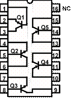
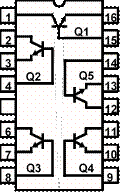
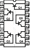
HFA3096, HFA3127, HFA3128

HFA3046
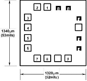
Pad numbers correspond to package part pin out.
 |
1 2 3 4 5
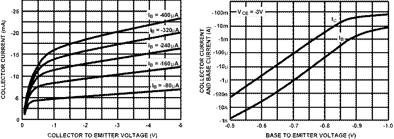
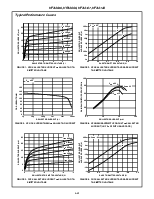
COLLECTOR TO EMITTER VOLTAGE (V)
COLLECTOR CURRENT (A)
0.5 0.6 0.7 0.8 0.9 1.0
BASE TO EMITTER VOLTAGE (V)
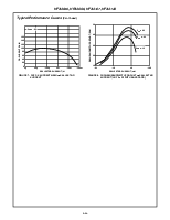
Typical Performance Curves(Continued)
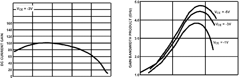
-1µ -10µ -100µ -1m -10m -100m -0.1 -1.0 -10 -100
COLLECTOR CURRENT (A) COLLECTOR CURRENT (mA)
Уважаемый посетитель!
Чтобы распечатать файл, скачайте его (в формате Word).
Ссылка на скачивание - внизу страницы.
 NC
NC
 5 NC
5 NC
 5
5