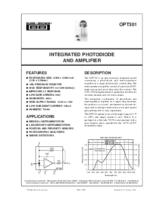
transimpedance amplifier on a single chip eliminates ● LOW QUIESCENT CURRENT: 400µA the problems commonly encountered in discrete de- signs such as leakage current errors, noise pick-up and ● HERMETIC TO-99 gain peaking due to stray capacitance. The OPT301 operates over a wide supply range (±2.25 APPLICATIONS to ±18V) and supply current is only 400µA. It is packaged in a hermetic TO-99 metal package with a ● MEDICAL INSTRUMENTATION glass window, and is specified for the –40°C to 85°C ● LABORATORY INSTRUMENTATION temperature range. ● POSITION AND PROXIMITY SENSORS ● PHOTOGRAPHIC ANALYZERS ● SMOKE DETECTORS
International Airport Industrial Park • Mailing Address: PO Box 11400, Tucson, AZ 85734 • Street Address: 6730 S. Tucson Blvd., Tucson, AZ 85706 • Tel: (520) 746-1111 • Twx: 910-952-1111 Internet: http://www.burr-brown.com/ • FAXLine: (800) 548-6133 (US/Canada Only) • Cable: BBRCORP • Telex: 066-6491 • FAX: (520) 889-1510 • Immediate Product Info: (800) 548-6132 |
©
1994 Burr-Brown Corporation PDS-1228B Printed in U.S.A. January, 1994
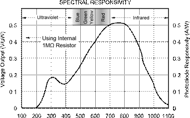
At TA = +25°C, VS = ±15V, λ = 650nm, internal 1MΩ feedback resistor, unless otherwise noted.
|
PARAMETER |
CONDITIONS |
OPT301M |
UNITS |
||
|
MIN |
TYP |
MAX |
|||
|
RESPONSIVITY Photodiode Current |
650nm |
0.47 |
A/W |
||
|
Voltage Output |
650nm |
0.47 |
V/µW |
||
|
vs Temperature |
200 |
ppm/°C |
|||
|
Unit-to-Unit Variation |
650nm |
±5 |
% |
||
|
Nonlinearity(1) |
FS Output = 10V |
0.01 |
% of FS |
||
|
Photodiode Area |
(0.090 x 0.090in) |
0.008 |
in2 |
||
|
(2.29 x 2.29mm) |
5.2 |
mm2 |
|||
|
DARK ERRORS, RTO(2) Offset Voltage, Output |
±0.5 |
±2 |
mV |
||
|
vs Temperature |
±10 |
µV/°C |
|||
|
vs Power Supply |
VS = ±2.25V to ±18V |
10 |
100 |
µV/V |
|
|
Voltage Noise |
Measured BW = 0.1 to 100kHz |
160 |
µVrms |
||
|
RESISTOR—1MΩ Internal Resistance |
1 |
MΩ |
|||
|
Tolerance |
±0.5 |
±2 |
% |
||
|
vs Temperature |
50 |
ppm/°C |
|||
|
FREQUENCY RESPONSE Bandwidth, Large or Small-Signal, –3dB |
4 |
kHz |
|||
|
Rise Time, 10% to 90% |
90 |
µs |
|||
|
Settling Time, 1% |
FS to Dark |
240 |
µs |
||
|
0.1% |
FS to Dark |
350 |
µs |
||
|
0.01% |
FS to Dark |
900 |
µs |
||
|
Overload Recovery Time |
100% overdrive, VS = ±15V |
240 |
µs |
||
|
100% overdrive, VS = ±5V |
500 |
µs |
|||
|
100% overdrive, VS = ±2.25V |
1000 |
µs |
|||
|
OUTPUT Voltage Output |
RL = 10kΩ |
(V+) – 1.25 |
(V+) – 0.65 |
V |
|
|
RL = 5kΩ |
(V+) – 2 |
(V+) – 1 |
V |
||
|
Capacitive Load, Stable Operation |
10 |
nF |
|||
|
Short-Circuit Current |
±18 |
mA |
|||
|
POWER SUPPLY Specified Operating Voltage |
±15 |
V |
|||
|
Operating Voltage Range |
±2.25 |
±18 |
V |
||
|
Quiescent Current |
IO = 0 |
±0.4 |
±0.5 |
mA |
|
|
TEMPERATURE RANGE Specification |
–40 |
+85 |
°C |
||
|
Operating/Storage |
–55 |
+125 |
°C |
||
|
Thermal Resistance, θJA |
200 |
°C/W |
NOTES: (1) Deviation in percent of full scale from best-fit straight line. (2) Referred to Output. Includes all error sources.
At TA = +25°C, unless otherwise noted.
|
PARAMETER |
CONDITIONS |
Photodiode of OPT30 |
1 |
UNITS |
|
|
MIN |
TYP |
MAX |
|||
|
Photodiode Area |
(0.090 x 0.090in) |
0.008 |
in2 |
||
|
(2.29 x 2.29mm) |
5.1 |
mm2 |
|||
|
Current Responsivity |
650nm |
0.47 |
A/W |
||
|
Dark Current |
VD = 0V(1) |
500 |
fA |
||
|
vs Temperature |
doubles every 10°C |
||||
|
Capacitance |
VD = 0V(1) |
4000 |
pF |
NOTE: (1) Voltage Across Photodiode.
|
PARAMETER |
CONDITIONS |
OPT301 Op Amp |
UNITS |
||||
|
MIN |
TYP |
MAX |
|||||
|
INPUT Offset Voltage vs Temperature vs Power Supply Input Bias Current vs Temperature |
VS = ±2.25V to ±18V |
±0.5 ±5 10 1 doubles every 10°C |
mV µV/°C µV/V pA |
||||
|
NOISE Input Voltage Noise Voltage Noise Density, f=10Hz f=100Hz f=1kHz Current Noise Density, f=1kHz |
30 25 15 0.8 |
|
|||||
|
INPUT VOLTAGE RANGE Common-Mode Input Range Common-Mode Rejection |
±14.4 106 |
V dB |
|||||
|
INPUT IMPEDANCE Differential Common-Mode |
1012||3 1012||3 |
Ω||pF Ω||pF |
|||||
|
OPEN-LOOP GAIN Open-Loop Voltage Gain |
120 |
dB |
|||||
|
FREQUENCY RESPONSE Gain-Bandwidth Product Slew Rate Settling Time 0.1% 0.01% |
380 0.5 4 5 |
kHz V/µs µs µs |
|||||
|
6 |
|||||||
|
OUTPUT Voltage Output |
RL = 10kΩ |
(V+) – 1.25 |
(V+) – 0.65 |
V |
|||
|
RL = 5kΩ |
(V+) – 2 |
(V+) – 1 |
V |
||||
|
Short-Circuit Current |
±18 |
mA |
|||||
|
POWER SUPPLY Specified Operating Voltage |
±15 |
V |
|||||
|
Operating Voltage Range |
±2.25 |
±18 |
V |
||||
|
Quiescent Current |
IO = 0 |
±0.4 |
±0.5 |
mA |
|||
At TA = +25°C, VS = ±15V, unless otherwise noted.
NOTE: (1) Op amp specifications provided for information and comparison only.
The information provided herein is believed to be reliable; however, BURR-BROWN assumes no responsibility for inaccuracies or omissions. BURR-BROWN assumes no responsibility for the use of this information, and all use of such information shall be entirely at the user’s own risk. Prices and specifications are subject to change without notice. No patent rights or licenses to any of the circuits described herein are implied or granted to any third party. BURR-BROWN does not authorize or warrant any BURR-BROWN product for use in life support devices and/or systems.
|
PACKAGE DRAWING |
||
|
PRODUCT |
PACKAGE |
NUMBER(1) |
|
OPT301M |
8-Pin TO-99 |
001-1 |
 ELECTROSTATIC
DISCHARGE SENSITIVITY
ELECTROSTATIC
DISCHARGE SENSITIVITYThis integrated circuit can be damaged by ESD. Burr-Brown recommends that all integrated circuits be handled with appropriate precautions. Failure to observe proper handling and installation procedures can cause damage.
ESD damage can range from subtle performance degradation to complete device failure. Precision integrated circuits may be more susceptible to damage because very small parametric changes could cause the device not to meet its published
PACKAGE INFORMATION
|
Supply Voltage ................................................................................... ±18V Input Voltage Range (Common Pin) .................................................... ±VS Output Short-Circuit (to ground)............................................... Continuous Operating Temperature................................................... –55°C to +125°C Storage Temperature ...................................................... –55°C to +125°C Junction Temperature .................................................................... +125°C Lead Temperature (soldering, 10s)................................................ +300°C |
NOTE: (1) For detailed drawing and dimension table, please see end of data sheet, or Appendix C of Burr-Brown IC Data Book.
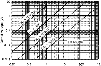
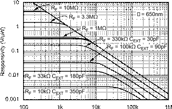
At TA = +25°C, VS = ±15V, λ = 650nm, unless otherwise noted.

Wavelength (nm)
 |
Radiant Power (µW)

|
6 |
Irradiance (W/m2)
DISTRIBUTION OF RESPONSIVITY

Responsivity (A/W)
Frequency (Hz)

0 ±20 ±40 ±60 ±80
Incident Angle (°)
At TA = +25°C, VS = ±15V, λ = 650nm, unless otherwise noted.
OUTPUT NOISE VOLTAGE
QUIESCENT CURRENT vs TEMPERATURE vs MEASUREMENT BANDWIDTH
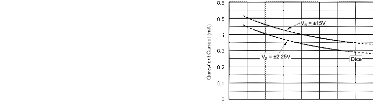
–75 –50 –25 0 25 50 75 100 125 1 10 100 1k 10k 100k
SMALL-SIGNAL DYNAMIC RESPONSE LARGE-SIGNAL DYNAMIC RESPONSE
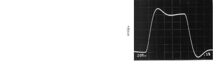
100µs/div 100µs/div

Measurement Bandwidth (Hz)
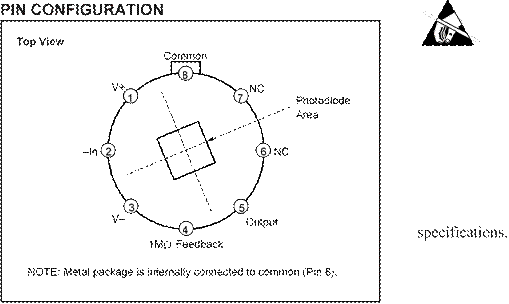
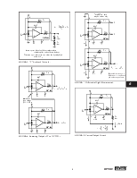
Figure 1 shows the basic connections required to operate the OPT301. Applications with high-impedance power supplies may require decoupling capacitors located close to the device pins as shown. Output is zero volts with no light and increases with increasing illumination.
If your light source is focused to a small area, be sure that it is properly aimed to fall on the photodiode. If a narrowly focused light source were to miss the photodiode area and fall only on the op amp circuitry, the OPT301 would not perform properly. The large (0.090 x 0.090 inch) photodiode area allows easy positioning of narrowly focused light sources. The photodiode area is easily visible—it appears

FIGURE 1. Basic Circuit Connections.
Photodiode current, ID, is proportional to the radiant power or flux (in watts) falling on the photodiode. At a wavelength of 650nm (visible red) the photodiode Responsivity, RI, is approximately 0.45A/W. Responsivity at other wavelengths very dark compared
Уважаемый посетитель!
Чтобы распечатать файл, скачайте его (в формате Word).
Ссылка на скачивание - внизу страницы.
 Wavelength
(nm)
Wavelength
(nm)