
DC to DC Converters Using ®
TOPSwitch®for Telecom and
Cablecom Applications
Design Note DN-16
 The TOPSwitch
product family provides a cost effective and reliable solution for DC to DC
converter applications. The TOP100-TOP104 series of products can be used for
input voltages as low as 16VDC and as high as 200VDC in a flyback topology.
The 350V breakdown voltage minimizes primary clamping requirements in low
voltage applications, reducing cost and simplifying the design. The high level
of system integration reduces component count and board space while boosting
power density. Because TOPSwitch is very easy to use, design time to
production is greatly reduced. Compared to discrete PWM and converter modules,
the TOPSwitch solution reduces total cost, component count, size, and
weight while also increasing system reliability.
The TOPSwitch
product family provides a cost effective and reliable solution for DC to DC
converter applications. The TOP100-TOP104 series of products can be used for
input voltages as low as 16VDC and as high as 200VDC in a flyback topology.
The 350V breakdown voltage minimizes primary clamping requirements in low
voltage applications, reducing cost and simplifying the design. The high level
of system integration reduces component count and board space while boosting
power density. Because TOPSwitch is very easy to use, design time to
production is greatly reduced. Compared to discrete PWM and converter modules,
the TOPSwitch solution reduces total cost, component count, size, and
weight while also increasing system reliability.
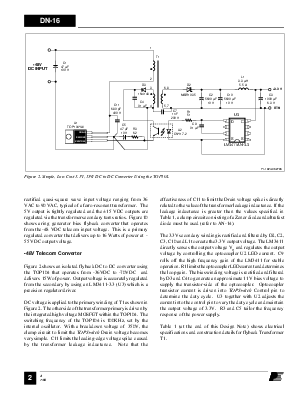
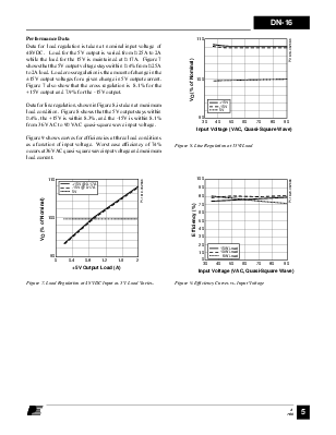
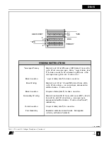
Output power ranges for each TOPSwitch as a function of DC input voltage are shown in the table below. For each minimum input voltage value shown, an output power range is given for each TOPSwitch for an expected converter efficiency of approximately 80% with losses split evenly between TOPSwitch and the rest of the circuitry. The transformer should be designed for the indicated reflected voltage VOR and will have maximum duty cycle DMAX approaching 64%. Refer to Application Note AN-17 for more information on reflected voltage and transformer design.
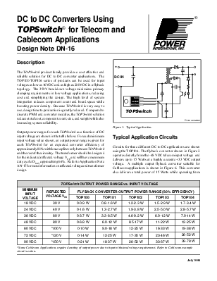
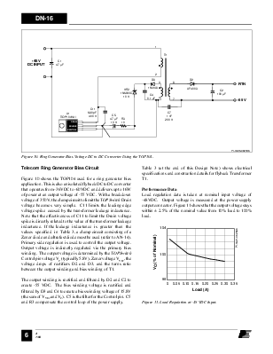
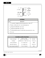
+
DC IN
-
DRAIN
SOURCE
CONTROL
PI-1914-062696
Figure 1. Typical Application.
Circuits for three different DC to DC applications are shown using the TOP104. The flyback converter shown in Figure 2 operates directly from the -48 VDC telecom input voltage and delivers up to 15 Watts at a highly accurate +3.3 VDC output voltage. A multiple output flyback converter suitable for Cablecom applications is shown in Figure 6. This converter also delivers a total power of 15 Watts while operating from
|
TOPSwitch OUTPUT POWER RANGE vs. INPUT VOLTAGE |
||||||
|
MINIMUM INPUT VOLTAGE |
REFLECTED VOLTAGE VOR |
FLYBACK CONVERTER OUTPUT POWER RANGE (80% EFFICIENCY) |
||||
|
TOP100 |
TOP101 |
TOP102 |
TOP103 |
TOP104 |
||
|
18 VDC |
30 V |
0-0.9 W |
0.8-1.6 W |
1.2-2.3 W |
1.5-2.9 W |
1.7-3.4 W |
|
24 VDC |
40 V |
0-1.6 W |
1.3-2.7 W |
1.9-3.8 W |
2.5-5.0 W |
2.8-5.7 W |
|
36 VDC |
60 V |
0-3.7 W |
3.3-6.5 W |
4.6-9.2 W |
6.0-12 W |
7.0-14 W |
|
48 VDC |
80 V |
0-6.8 W |
6.0-12 W |
8.5-17 W |
11-22 W |
12-25 W |
|
60 VDC |
*100 V |
0-10 W |
9.0-18 W |
12-25 W |
16-33 W |
19-38 W |
|
72 VDC |
*120 V |
0-14 W |
12-25 W |
17-35 W |
23-46 W |
26-52 W |
|
90 VDC |
*150 V |
0-21 W |
18-37 W |
26-52 W |
33-67 W |
39-78 W |
*Some Cablecom Applications require derating of output power due to input withstand voltage requirement. Refer to Cablecom example circuit section.
![]()
July 1996
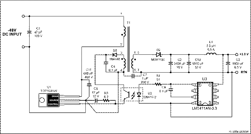
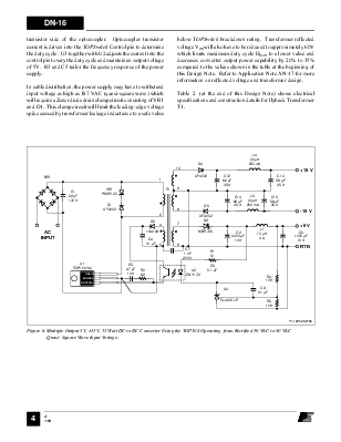
Figure 2. Simple, Low Cost 3.3V, 15W DC to DC Converter Using the TOP104.
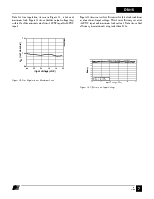
rectified quasi-square wave input voltage ranging from 36 VAC to 90 VAC, typical of a ferro-resonant transformer. The 5V output is tightly regulated and the ±15 VDC outputs are regulated via the transformer secondary turns ratios. Figure 10 shows a ring generator bias flyback converter that operates from the -48 VDC telecom input voltage. This is a primary regulated converter that delivers up to 16 Watts of power at 55 VDC output voltage.
-48V Telecom Converter
Figure 2 shows an isolated flyback DC to DC converter using the TOP104 that operates from -36VDC to -70VDC and delivers 15W of power. Output voltage is accurately regulated from the secondary by using an LM3411-3.3 (U3) which is a precision regulator/driver.
DC voltage is applied to the primary winding of T1 as shown in Figure 2. The other side of the transformer primary is driven by the integrated high voltage MOSFET within the TOP104. The switching frequency of the TOP104 is 100KHz, set by the internal oscillator. With a breakdown voltage of 350V, the clamp circuit to limit the TOPSwitch Drain voltage becomes very simple. C11 limits the leading-edge voltage spike caused by the transformer leakage inductance. Note that the effectiveness of C11 to limit the Drain voltage spike is directly related to the value of the transformer leakage inductance. If the leakage inductance is greater than the values specified in Table 1, a clamp circuit consisting of a Zener diode and ultrafast diode must be used (refer to AN-14).
The 3.3V secondary winding is rectified and filtered by D2, C2, C3, C10 and L1 to create the 3.3 V output voltage. The LM3411 directly senses the output voltage VO and regulates
Уважаемый посетитель!
Чтобы распечатать файл, скачайте его (в формате Word).
Ссылка на скачивание - внизу страницы.