|
Philips Semiconductors |
Product specification |
|
|
Triacs |
BT136F series |
|
|
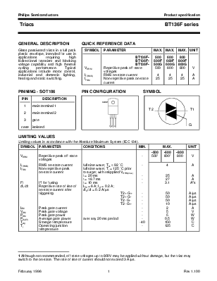
GENERAL DESCRIPTION |
QUICK REFERENCE DATA |
|
SYMBOL |
PARAMETER
BT136F- |
MAX.
500 |
MAX.
600 |
MAX.
800 |
UNIT
|
|
BT136F- |
500F |
600F |
800F |
||
|
BT136F- |
500G |
600G |
800G |
||
|
VDRM |
Repetitive peak off-state voltages |
500 |
600 |
800 |
V |
|
IT(RMS) |
RMS on-state current |
4 |
4 |
4 |
A |
|
ITSM |
Non-repetitive peak on-state current |
25 |
25 |
25 |
A |
Glass passivated triacs in a full pack plastic envelope, intended for use in applications requiring high bidirectional transient and blocking voltage capability and high thermal cycling performance. Typical applications include motor control, industrial and domestic lighting, heating and static switching.
|
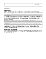
PINNING - SOT186 |
PIN CONFIGURATION |
SYMBOL |
||||||||||||
|
|
|||||||||||||
Limiting values in accordance with the Absolute Maximum System (IEC 134).
|
SYMBOL |
PARAMETER |
CONDITIONS |
MIN. |
MAX. |
UNIT |
||
|
-500 |
-600 |
-800 |
|||||
|
VDRM |
Repetitive peak off-state |
- |
500[1] |
6001 |
800 |
V |
|
|
IT(RMS) |
voltages RMS on-state current |
full sine wave; Ths ≤ 92 ˚C |
- |
A |
|||
|
4 |
|||||||
|
ITSM |
Non-repetitive peak |
full sine wave; Tj = 125 ˚C prior |
|||||
|
on-state current |
to surge; with reapplied VDRM(max) t = 20 ms |
- |
25 |
A |
|||
|
t = 16.7 ms |
- |
27 |
A |
||||
|
I2t |
I2t for fusing |
t = 10 ms |
- |
3.1 |
A2s |
||
|
dIT/dt |
Repetitive rate of rise of |
ITM = 6 A; IG = 0.2 A; |
|||||
|
on-state current after |
dIG/dt = 0.2 A/µs |
||||||
|
triggering |
T2+ G+ |
- |
50 |
A/µs |
|||
|
T2+ G- |
- |
50 |
A/µs |
||||
|
T2- G- |
- |
50 |
A/µs |
||||
|
T2- G+ |
- |
10 |
A/µs |
||||
|
IGM |
Peak gate current |
- |
2 |
A |
|||
|
VGM |
Peak gate voltage |
- |
5 |
V |
|||
|
PGM |
Peak gate power |
- |
5 |
W |
|||
|
PG(AV) |
Average gate power |
over any 20 ms period |
- |
0.5 |
W |
||
|
Tstg |
Storage temperature |
-40 |
150 |
˚C |
|||
|
Tj |
Operating junction temperature |
- |
125 |
˚C |
Ths = 25 ˚C unless otherwise specified
|
SYMBOL |
PARAMETER |
CONDITIONS |
MIN. |
TYP. |
MAX. |
UNIT |
|
Visol |
Repetitive peak voltage from all three terminals to external heatsink |
R.H. ≤ 65% ; clean and dustfree |
- |
1500 |
V |
|
|
Cisol |
Capacitance from T2 to external heatsink |
f = 1 MHz |
- |
12 |
- |
pF |
|
SYMBOL |
PARAMETER |
CONDITIONS |
MIN. |
TYP. |
MAX. |
UNIT |
|
Rth j-hs |
Thermal resistance |
full or half cycle |
||||
|
junction to heatsink |
with heatsink compound |
- |
- |
5.5 |
K/W |
|
|
without heatsink compound |
- |
- |
7.2 |
K/W |
||
|
Rth j-a |
Thermal resistance junction to ambient |
in free air |
- |
55 |
- |
K/W |
Tj = 25 ˚C unless otherwise stated
|
SYMBOL |
PARAMETER |
CONDITIONS |
MIN. |
TYP. |
MAX. |
UNIT |
||
|
BT136F- |
... |
...F |
...G |
|||||
|
IGT |
Gate trigger current |
VD = 12 V; IT = 0.1 A T2+ G+ |
- |
5 |
35 |
25 |
50 |
mA |
|
T2+ G- |
- |
8 |
35 |
25 |
50 |
mA |
||
|
T2- G- |
- |
11 |
35 |
25 |
50 |
mA |
||
|
T2- G+ |
- |
30 |
70 |
70 |
100 |
mA |
||
|
IL |
Latching current |
VD = 12 V; IGT = 0.1 A T2+ G+ |
- |
7 |
20 |
20 |
30 |
mA |
|
T2+ G- |
- |
16 |
30 |
30 |
45 |
mA |
||
|
T2- G- |
- |
5 |
20 |
20 |
30 |
mA |
||
|
T2- G+ |
- |
7 |
30 |
30 |
45 |
mA |
||
|
IH VT |
Holding current On-state voltage |
VD = 12 V; IGT = 0.1 A IT = 5 A |
- - |
5 1.4 |
15 |
15 |
30 |
mA V |
|
1.70 |
||||||||
|
VGT |
Gate trigger voltage |
VD = 12 V; IT = 0.1 A |
- |
0.7 |
1.5 |
V |
||
|
VD = 400 V; IT = 0.1 A; Tj = 125 ˚C |
0.25 |
0.4 |
- |
V |
||||
|
ID |
Off-state leakage current |
VD = VDRM(max); Tj = 125 ˚C |
- |
0.1 |
0.5 |
mA |
 Tj
= 25 ˚C unless otherwise stated
Tj
= 25 ˚C unless otherwise stated
|
SYMBOL |
PARAMETER |
CONDITIONS |
MIN. |
TYP. |
MAX. |
UNIT |
||
|
BT136F- |
... |
...F |
...G |
|||||
|
dVD/dt |
Critical rate of rise of |
VDM = 67% VDRM(max)V; |
100 |
50 |
200 |
250 |
- |
V/µs |
|
off-state voltage |
Tj = 125 ˚C; exponential waveform; gate open circuit |
|||||||
|
dVcom/dt |
Critical rate of change of |
VDM = 400 V; Tj = 95 ˚C; |
- |
- |
10 |
50 |
- |
V/µs |
|
commutating voltage |
IT(RMS) = 4 A; dIcom/dt = 1.8 A/ms; gate open circuit |
|||||||
|
tgt |
Gate controlled turn-on |
ITM = 6 A; VD = VDRM(max); |
- |
- |
- |
2 |
- |
µs |
|
time |
IG = 0.1 A; dIG/dt = 5 A/µs |
0 1 2 3 4 5
IT(RMS) / A
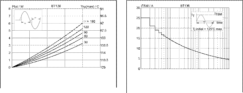
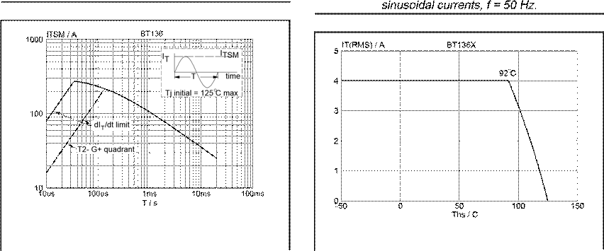 Fig.1.
Maximum on-state dissipation, Ptot, versus rms on-state current, IT(RMS), where α = conduction angle.
Fig.1.
Maximum on-state dissipation, Ptot, versus rms on-state current, IT(RMS), where α = conduction angle.
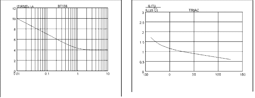
Fig.2. Maximum permissible non-repetitive peak on-state current ITSM, versus pulse width tp, for sinusoidal currents, tp ≤ 20ms.
1 10 100 1000 Number of cycles at 50Hz
Fig.3. Maximum permissible non-repetitive peak on-state current ITSM, versus number of cycles, for
surge duration / s Tj / C
Fig.5. Maximum permissible
repetitive rms on-state Fig.8. Normalised latching current IL(Tj)/ IL(25˚C), current IT(RMS), versus surge
duration, for sinusoidal versus junction temperature Tj. 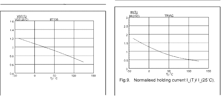 currents, f = 50
Hz; T ≤ 92˚C.
currents, f = 50
Hz; T ≤ 92˚C.
VGT(Tj)/ VGT(25˚C), versus junction temperature Tj.
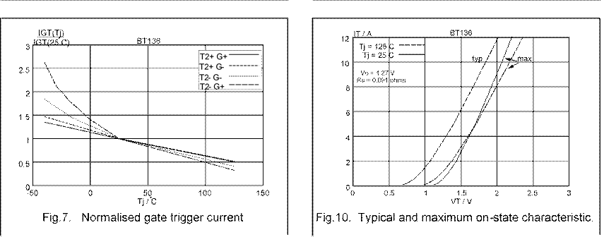
IGT(Tj)/ IGT(25˚C), versus junction temperature Tj.
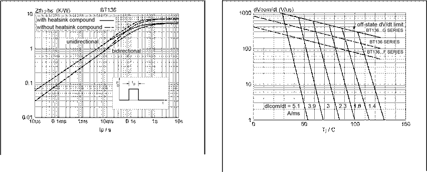 Fig.11.
Transient thermal impedance Zth j-hs, versus pulse
Fig.11.
Transient thermal impedance Zth j-hs, versus pulse
Уважаемый посетитель!
Чтобы распечатать файл, скачайте его (в формате Word).
Ссылка на скачивание - внизу страницы.