 HFA3127/883
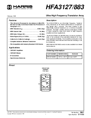
February 1995 Ultra High Frequency Transistor Array
|
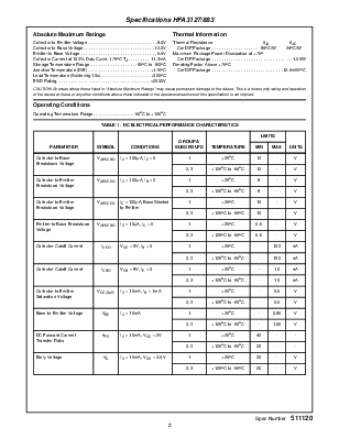
Features Description • This Circuit is Processed in Accordance to MIL-STD- The HFA3127/883 is an Ultra High Frequency Transistor 883 and is Fully Conformant Under the Provisions of Array fabricated on the Harris Semiconductor complemenParagraph 1.2.1. tary bipolar UHF-1 process. This array consists of five dielectrically isolated transistors on a common monolithic • NPN Transistor (fT). . . . . . . . . . . . . . . . . . . . .8GHz (Typ) substrate. The high fT (8GHz) and low noise figure (3.5dB) • NPN Current Gain . . . . . . . . . . . . . . . . . . . . . . . 40 (Min) of these transistors make them ideal for high frequency amplifier and mixer applications. • NPN Early Voltage (VA) . . . . . . . . . . . . . . . . . . . 20 (Min) The HFA3127/883 is an all-NPN array. Access is provided to • Noise Figure (50Ω) at 1.0GHz . . . . . . . . . . . 3.5dB (Typ) each of the terminals of the individual transistors for maxi• Collector-to-Collector Leakage. . . . . . . . . . .<1pA (Typ) mum application flexibility. The monolithic construction of the array provides close electrical and thermal matching of the • Complete Isolation Between Transistors five transistors. • Pin Compatible with Industry Standard 3XXX Series SMD 5962-9474901MEA version is also available from Harris Semiconductor. Applications
• VHF/UHF Amplifiers Ordering Information
• VHF/UHF Mixers • IF Converters • Synchronous Detectors
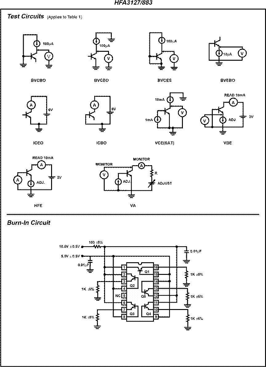
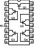
Pinout HFA3127/883 (CERDIP) TOP VIEW
|
CAUTION: These devices are sensitive to electrostatic discharge. Users should follow proper I.C. Handling Procedures. File Number 3967
Copyright © Harris Corporation 1995
Spec Number 511120
|
Absolute Maximum Ratings Thermal Information Collector to Emitter Voltage . . . . . . . . . . . . . . . . . . . . . . . . . . . .8.0V Thermal Resistance θJA θJC Collector to Base Voltage. . . . . . . . . . . . . . . . . . . . . . . . . . . . .12.0V CerDIP Package . . . . . . . . . . . . . . . . . . . 80oC/W 24oC/W Emitter to Base Voltage . . . . . . . . . . . . . . . . . . . . . . . . . . . . . . .5.5V Maximum Package Power Dissipation at +75 o Collector Current at 100% Duty Cycle, 175oC TJ. . . . . . . . . 11.3mA CerDIP Package . . . . . . . . . . . . . . . . . . . . . . . . . . . . . . . . . 1.25W Storage Temperature Range . . . . . . . . . . . . . . . . . . -65oC to 150oC Derating Factor Above +75oC Junction Temperature (DIE) . . . . . . . . . . . . . . . . . . . . . . . . . +175oC CerDIP Package . . . . . . . . . . . . . . . . . . . . . . . . . . . . .12.5mW/oC Lead Temperature (Soldering 10s). . . . . . . . . . . . . . . . . . . . +300oC ESD Rating. . . . . . . . . . . . . . . . . . . . . . . . . . . . . . . . . . . . . . <2000V CAUTION: Stresses above those listed in “Absolute Maximum Ratings” may cause permanent damage to the device. This is a stress only rating and operation of the device at these or any other conditions above those indicated in the operational sections of this specification is not implied.
Operating Conditions Operating Temperature Range. . . . . . . . . . . . . . . . -55oC to +125oC
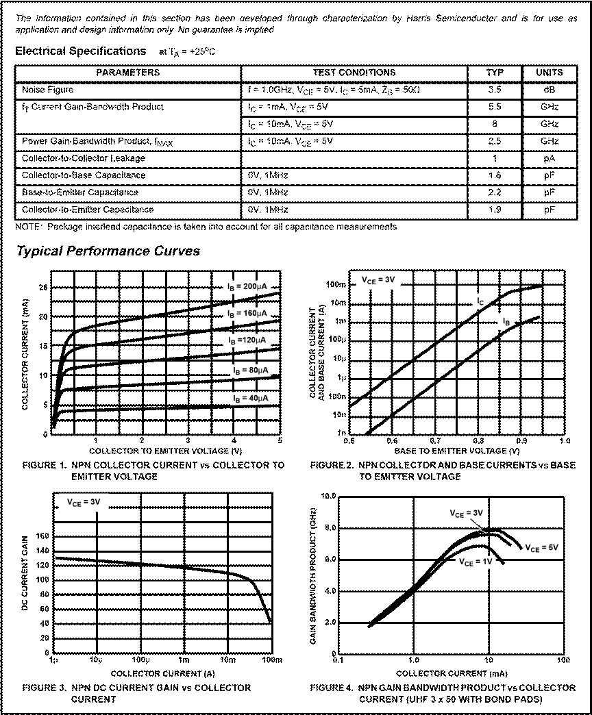
TABLE 1. DC ELECTRICAL PERFORMANCE CHARACTERISTICS
|
||||||||||||||||||||||||||||||||||||||||||||||||||||||||||||||||||||||||||||||||||||||||||||||||||||||||||||||||||||||||||||||||||||||||||||
|
TABLE 2. ELECTRICAL PERFORMANCE CHARACTERISTICS Table 2 Intentionally Left Blank. TABLE 3. ELECTRICAL PERFORMANCE CHARACTERISTICS Table 3 Intentionally Left Blank. TABLE 4. ELECTRICAL TEST REQUIREMENTS
NOTE: 1. PDA applies to Subgroup 1 only. |
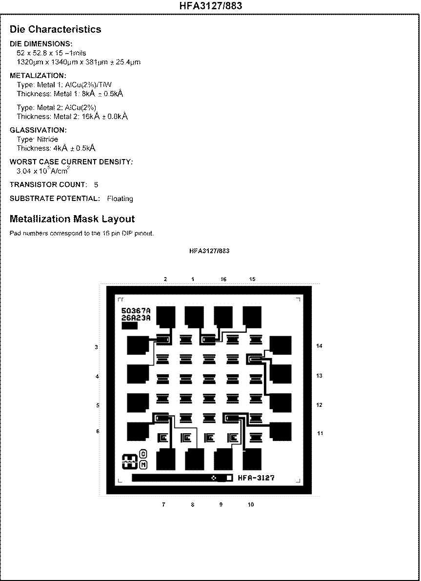
HFA3127
DESIGN INFORMATION
February 1995 Ultra High Frequency Transistor Array
|
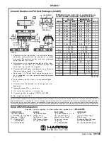
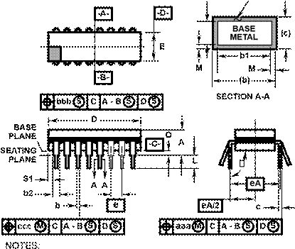
Ceramic Dual-In-Line Frit Seal Packages (CerDIP)
c1 LEAD
FINISH F16.3
MIL-STD-1835
GDIP1-T16 (D-2, CONFIGURATION A) 1. Index area: A notch or a pin one identification mark shall be located adjacent to pin one and shall be located within the shaded area shown. The manufacturer’s identification shall not be used as a pin one identification mark. 2. The maximum limits of lead dimensions b and c or M shall bemeasured at the centroid of the finished lead surfaces, when solder dip or tin plate lead finish is applied. 3. Dimensions b1 and c1 apply to lead base metal only. DimensionM applies to lead plating and finish thickness. 4. Corner leads (1, N, N/2, and N/2+1) may be configured with a partial lead paddle. For this configuration dimension b3 replaces dimension b2. Rev. 0 4/94 5. This dimension allows for off-center lid, meniscus, and glassoverrun. 6. Dimension Q shall be measured from the seating plane to thebase plane. 7. Measure dimension S1 at all four corners. 8. N is the maximum number of terminal positions. 9. Dimensioning and tolerancing per ANSI Y14.5M - 1982. 10. Controlling dimension: INCH.
Harris Semiconductor products are sold by description only. Harris Semiconductor reserves the right to make changes in circuit design and/or specifications at any time without notice. Accordingly, the reader is cautioned to verify that data sheets are current before placing orders. Information furnished by Harris is believed to be accurate and reliable. However, no responsibility is assumed by Harris or its subsidiaries for its use; nor for any infringements of patents or other rights of third parties which may result from its use. No license is granted by implication or otherwise under any patent or patent rights of Harris or its subsidiaries.
Sales Office Headquarters For general information regarding Harris Semiconductor and its products, call 1-800-4-HARRIS UNITED STATES EUROPE SOUTH ASIA NORTH ASIA Harris Semiconductor Harris Semiconductor Harris Semiconductor H.K. Ltd. Harris K.K. P. O. Box 883, Mail Stop 53-210 Mercure Center 13/F Fourseas Building Kojimachi-Nakata Bldg. 4F Melbourne, FL 32902 100, Rue de la Fusee 208-212 Nathan Road 5-3-5 Kojimachi TEL: 1-800-442-7747 1130 Brussels, Belgium Tsimshatsui, Kowloon Chiyoda-ku, Tokyo 102 Japan (407) 729-4984 TEL: (32) 2-724-2111 Hong Kong TEL: (81) 3-3265-7571 FAX: (407) 729-5321 TEL: (852) 723-6339 TEL: (81) 3-3265-7572 (Sales | ||||||||||||||||||||||||||||||||||||||||||||||||||||||||||||||||||||||||||||||||||||||||||||||||||||||||||||||||||||||||||||||||||||||||
Уважаемый посетитель!
Чтобы распечатать файл, скачайте его (в формате Word).
Ссылка на скачивание - внизу страницы.
 16
LEAD CERAMIC DUAL-IN-LINE FRIT SEAL PACKAGE
16
LEAD CERAMIC DUAL-IN-LINE FRIT SEAL PACKAGE