
TOSHIBA BIPOLAR DIGITAL INTEGRATED CIRCUIT CIRCUIT SILICON MONOLITHIC
FREQUENCY SYNTHESIZER FOR TV / CATV
|
TD6358P
DIP20-P-300-2.54A TD6358N
SDIP20-P-300-1.78 |
|
Simple control bus • 19bit serial input |
Weight |
|
|
5V single power supply operation |
DIP20-P-300-2.54A SDIP20-P-300-1.78 |
• 2.25g (Typ.) • 1.029 (Typ.) |
![]()
![]() The TD6358P
and TD6358N are single-chip frequency synthesizer ICs, which can organization
high-performance frequency synthesizer systems in combination with a 4bit
"CPU controller.
The TD6358P
and TD6358N are single-chip frequency synthesizer ICs, which can organization
high-performance frequency synthesizer systems in combination with a 4bit
"CPU controller.
The TD6358P integrates high input sensitivity ECL prescaler, 1 2 L programmable counter, PI-L logic and bandswitch drive decoder in a DIP20-pin small package. The TD6358N is packaged in a shrink 20-pin package even smaller than TD6358P.
FEATURES
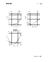
![]() High input sensitivity fin -80-100MHz : -24dBmW (500) (Min.) fin -O
I-IGHz : -27dBmW (500) (Min.)
High input sensitivity fin -80-100MHz : -24dBmW (500) (Min.) fin -O
I-IGHz : -27dBmW (500) (Min.)
![]() Wide operating
frequency IGHz (Max.)
Wide operating
frequency IGHz (Max.)
![]() 3.2MHz basic oscillator and 50kHz
frequency step
3.2MHz basic oscillator and 50kHz
frequency step
![]() Bandswitch driver 4
channels
Bandswitch driver 4
channels
(Note) Handle with care as this product is weak at surge voltage.
980910EBA1
|
'TOSHIBA is continually working to improve the quality and the reliability of its products. Nevertheless, semiconductor devices in general can malfunction or fail due to their inherent electrical sensitivity and vulnerability to physical stress. It is the responsibility of the buyer, when utilizing TOSHIBA products, to observe standards of safety, and to avoid situations in which a malfunction or failure of a TOSHIBA product could cause loss of human life, bodily injury or damage to property. In developing your designs, please ensure that TOSHIBA products are used within specified operating ranges as set forth in the most recent products specifications. Also, please keep in mind the precautions and conditions set forth in the TOSHIBA Semiconductor Reliability Handbook. 'The products described in this document are subject to the foreign exchange and foreign trade laws. 'The Information contained herein is presented only as a guide for the applications of our products. No responsibility is assumed by TOSHIBA CORPORATION for any infringements of intellectual property or other rights of the third parties which may result from its use. No license is granted by implication or otherwise under any intellectual property or other rights of TOSHIBA CORPORATION or others. The information contained herein is subject to change without notice. |
1/15
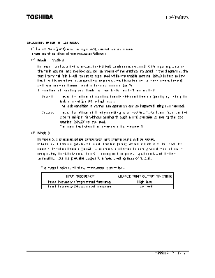
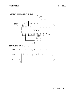
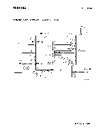
BLOCK DIAGRAM
![]()
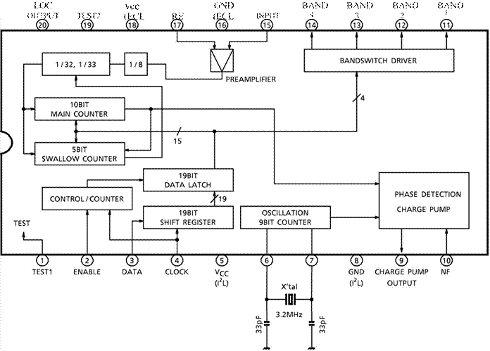 vcc GND
CHARGE PUMP
vcc GND
CHARGE PUMP(12L) (12L) OUTPUT
TERMINAL FUNCTION
|
PIN No. |
PIN NAME |
FUNCTION |
INTERFACE CIRCUIT |
|
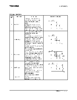
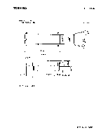
Test Pin 1 |
Low level : this will be in normal use operation mode when connected to GND or open. In order to prevent a static breakdown, it will be more effective to connect to GND. High level : this will be in test mode when connected to V |
|
|
|
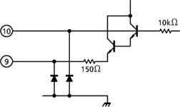
2 |
Enable Input |
This is an enable pulse input terminal at normal use operation. This will be a test mode select terminal of test mode by means of the pin 1 mode select pin. In order to prevent a static breakdown, it will be effective to connect in series a resistor of about 1kQ. The pins 3 and 4 below are the same as this pin. |
|
|
3 |
Data Input |
This is a data input terminal in normal mode. In test mode 1 or 2, this will be a main counter output terminal. In test mode 3, this can be an external input terminal of comparison signal of phase comparator (a counter output terminal in normal mode). |
|
|
4 |
Clock Input |
This is a clock pulse input terminal in normal mode. In test mode 1 or 2, this will be an output terminal of reference signal whose crystal oscillator is divided by 29 . In test mode 3, this can be an input terminal of external reference signal. |
|
|
5 |
Logic VCC |
This is logic circuit power supply. Connect a bypass condenser between this pin and pin 8. |
![]()
|
PIN No. |
PIN NAME |
FUNCTION |
INTERFACE CIRCUIT |
|
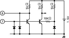
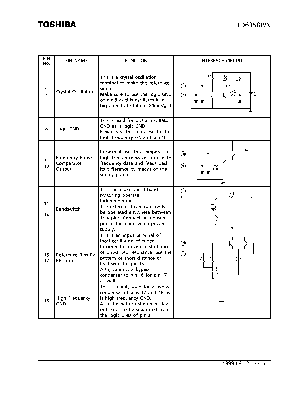
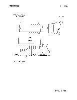
6 7 |
Crystal Oscillation |
This is a crystal oscillation terminal to make the reference signal. Make sure to use the logic GND of pin 8 as this oscillates in a big amplitude (about 800mVp-p). |
|
|
8 |
Logic GND |
This is used for crystal oscillator GND as is logic GND. Never wire this pin close to the high frequency GND of pin 16. |
|
|
9 10 |
Frequency Phase Comparator Output |
In normal use, this compares a high frequency wave input with frequency data and feeds back its difference by means of the supply pump. |
|
|
1 1
14 |
Bandswitch |
This can make the 4 band switching operate independently |
Уважаемый посетитель!
Чтобы распечатать файл, скачайте его (в формате Word).
Ссылка на скачивание - внизу страницы.
 20kQ
20kQ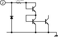 18kQ
18kQ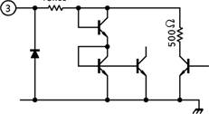 18kQ
18kQ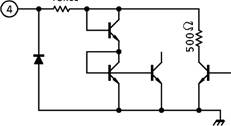 18kQ
18kQ