This allows the user to read the status register without changing its value.)
Write-one-to-clear (W1C) bits only can be cleared by writing one to them. Writing zero does not clear (or have any effect on) a W1C bit.
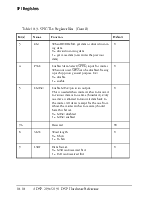
The following table provides the bit descriptions for the SPISTx register.
Table 10-6. SPISTx Register Bits
|
Bit |
Name |
Function |
Type |
Default |
|
0 |
SPIF |
This bit is set when an SPI single-word transfer is complete. |
RO |
1 |
|
1 |
MODF |
Mode-fault error. This bit is set in a master device when some other device tries to become the master. |
W1C |
0 |
Table 10-6. SPISTx Register Bits (Cont’d)
|
Bit |
Name |
Function |
Type |
Default |
|
2 |
TXE |
Transmission error. This bit is set when a transmission occurred with no new data in the TDBRx register. |
W1C |
0 |
|
3 |
TXS |
TDBRx data buffer status. 0 = empty 1 = full |
RO |
0 |
|
4 |
RBSY |
Receive error. This bit is set when data is received and the receive buffer is full. |
W1C |
0 |
|
5 |
RXS |
RX data buffer status. 0 = empty 1 = full |
RO |
0 |
|
6 |
TXCOL |
Transmit collision error. When this bit is set, corrupt data may have been transmitted. |
W1C |
0 |
The transmit buffer becomes full after it is written to; it becomes empty when a transfer begins and the transmit value is loaded into the shift register. The receive buffer becomes full at the end of a transfer when the shift register value is loaded into the receive buffer; it becomes empty when the receive buffer is read.
The Transmit Data Buffer Register (TDBRx) is a 16-bit read-write (RW) register. Data is loaded into this register before being transmitted. Just prior to the beginning of a data transfer, the data in TDBR is loaded into the Shift Data (SFDR) register. A normal core read of TDBRx can be done at any time and does not interfere with, or initiate, SPI transfers.
When the DMA is enabled for transmit operation, data is loaded into this register before being transmitted and then loaded into the shift register just prior to the beginning of a data transfer. A normal core write to TDBRx should not occur in this mode because this data will overwrite the DMA data to be transmitted.
When the DMA is enabled for receive operation, the contents of TDBRx will be repeatedly transmitted. A normal core write to TDBRx is permitted in this mode, and this data will be transmitted. If the “send zeroes” control bit (SZ) is set, TDBRx may be reset to 0 in certain circumstances.
If multiple writes to TDBRx occur while a transfer is already in progress, only the last data written will be transmitted; none of the intermediate values written to TDBRx will be transmitted. Multiple writes to TDBRx are possible but not recommended.
The Receive Data Buffer Register (RDBRx) is a 16-bit read-only (RO) register. At the end of a data transfer, the data in the shift register is loaded into RDBRx. During a DMA receive operation, the data in RDBRx is automatically read by the DMA. A shadow register for the receive data buffer, RDBRx, has been provided for use in debugging software. This register, RDBRSx, is at a different address from RDBRx, but its contents are identical to that of RDBRx. When a software read of RDBRx occurs, the RXS bit is cleared and an SPI transfer may be initiated (if TIMOD=00). No such hardware action occurs when the shadow register is read. RDBRSx is a read-only (RO) register.
The Data Shift Register (SFDR) is the 16-bit data shift register;
Уважаемый посетитель!
Чтобы распечатать файл, скачайте его (в формате Word).
Ссылка на скачивание - внизу страницы.