“Indirect Memory Read/Write—immediate premodify” on page 7-52
• “Indirect 16-bit Memory Write—immediate data” on page 7-55
• “Indirect 24-bit Memory Write—immediate data” on page 7-57
• “External IO Port Read/Write” on page 7-59
• “System Control Register Read/Write” on page 7-61
• “Modify Address Register—indirect” on page 7-63
• “Modify Address Register—direct” on page 7-65
This chapter describes each of the move instructions and the following related topics:
• “Core Registers” on page 7-2
• “PX Register” on page 7-4
• “DAG Registers” on page 7-6
• “Register Load Latencies” on page 7-9
• “Direct Addressing” on page 7-12
• “Indirect Addressing” on page 7-12
• “Circular Data Buffer Addressing” on page 7-15
• “Bit-Reversed Addressing” on page 7-17
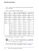
Table 7-1 lists the registers that reside in the DSP’s core. Most are 16-bit registers, but some Reg3 registers are shorter—ASTAT[9], MSTAT[7],
![]()
7-2 ADSP-219x Instruction Set Reference
Core Registers
SSTAT[8], LPCSTACKP[9], CCODE[4], PX[8], DMPG1[8], DMPG2[8], IOPG[8], IJPG[8], and STACKP[8].
Table 7-1. Core registers
|
Register Groups |
|||
|
Reg0 (Dreg) |
Reg1 (G1reg) |
Reg2 (G2reg) |
Reg3 (G3reg) |
|
AX0 |
I0 |
I4 |
ASTAT |
|
AX1 |
I1 |
I5 |
MSTAT |
|
MX0 |
I2 |
I6 |
SSTAT |
|
MX1 |
I3 |
I7 |
LPSTACKP |
|
AY0 |
M0 |
M4 |
CCODE |
|
AY1 |
M1 |
M5 |
SE |
|
MY0 |
M2 |
M6 |
SB |
|
MY1 |
M3 |
M7 |
PX |
|
MR2 |
L0 |
L4 |
DMPG1 |
|
SR2 |
L1 |
L5 |
DMPG2 |
|
AR |
L2 |
L6 |
IOPG |
|
SI |
L3 |
L7 |
IJPG |
|
MR1 |
IMASK |
Reserved |
Reserved |
|
SR1 |
IRPTL |
Reserved |
Reserved |
|
MR0 |
ICNTL |
CNTR |
Reserved |
|
SR0 |
STACKA |
LPSTACKA |
STACKP |
As shown, registers are grouped along functional lines:
• Reg0 (Dreg) Consists of data registers.
• Reg1 (G1reg) Consists of DAG1 addressing registers, interrupt
control registers, and the lower part of the PC stack register.
• Reg2 (G2reg) Consists of DAG2 addressing registers, the loop counter register, and the lower part of the loop PC register.
• Reg3 (G3reg) Consists of status registers, page registers.
The PX register, an 8-bit extension register, enables applications to transfer 24-bit data between 24-bit memory and 16-bit data registers. Only 24-bit accesses of 24-bit memory use the PX register. (So, a 16-bit read of 24-bit memory does not load the PX register, and a 16-bit write fills the lower eight bits in 24-bit memory with zeros (0).)
On reads, the PX register stores the lower eight bits of the 24-bit data transferring from memory to a destination register, and on writes, it supplies them for the data written to 24-bit data space.
Only two instructions use the PX register:
• ALU/MAC with dual indirect memory reads (see page “Compute with Dual Memory Read” on page 6-3)
• Indirect 24-bit memory read or write with pre- or postmodify addressing option (see page 7-37 and page 7-41)
![]()
7-4 ADSP-219x Instruction Set Reference
PX Register
To access 24-bit memory, you typically use the PM(Ireg += Mreg) syntax shown here:
AX1 = PM(I0 += M2); /* Read 24 bits, load 16 MSbits in AX1 */
/* PX autoloaded w/8 memory LSbits */
AY1 = PX; /* Load lower 8 bits from PX in AY1 */
PX = MR2; /* Load lower 8 bits into PX */
PM(I4 += M5) = MR1; /* Write all 24 bits from MR1 and PX */
On data reads using the PX register, the DSP transfers the upper sixteen bits of the 24-bit data to the destination data register and the lower eight bits to the PX register. The data loaded from memory is right-justified in the destination registers.
On data writes using the PX register, the DSP transfers the upper sixteen bits of the 24-bit data from the bus and the lower eight bits from the PX register, except for indirect writes of 24-bit immediate data, in which the instruction supplies the eight LSBs. The data written is right-justified in memory.
|
! |
PX transfers to and from memory occur automatically and transparently to the user, but the user must transfer data between the PX register and the data registers.
Because the DSP has a unified memory space, the address, not the syntax, determines whether the reference accesses 16-bit memory or 24-bit memory at run time.
• For 24-bit references that read 16-bit memory, the PX register receives whatever data the memory system outputs for the eight LSBs. For internal memory, this value is 0x00.
• For 24-bit references that write 16-bit memory, the DSP discards the data in the PX register.
The DAGs generate memory addresses for data transfers to and from memory. To do so, each uses a set of address registers and a page register. For fast context switching during interrupt servicing, the DAGs provide a secondary set of address registers. This section describes these registers.
Each DAG has a set of address registers that it uses to generate memory addresses for loading or storing data in memory. Each DAG can use its own set of address registers only. DAG1 uses registers 0 through 3, and DAG2 uses registers 4 through [1].
The DAG address registers are:
• Index (Ireg) Pointer to the current memory address. DAG1 (I0– I3); DAG2 (I4–I7).
• Modify (Mreg) Offset (from index) value for pre- or post-modify addressing. DAG1 (M0–M3); DAG2 (M4–M7).
• Length (Lreg) Number of memory locations in a buffer. DAG1 (L0–L3); DAG2 (L4–L7). For linear buffers, you must explicitly set Lreg = 0; for circular buffers, you must explicitly set Lreg to the length of the buffer.
• Base (Breg) Starting address of a circular buffer. DAG1 (B0–B3); DAG2 (B4–B7).Used with circular buffering only.
Each base (Breg) and length (Lreg) register is associated with its specific index (Ireg) register—I0/B0/L0, I1/B1/L1, …, and I7/B7/L7. So, although you can mix and match any of the index (Ireg) and modify
Уважаемый посетитель!
Чтобы распечатать файл, скачайте его (в формате Word).
Ссылка на скачивание - внизу страницы.