|
Symbol |
Condition |
Rating |
Unit |
||||
|
nin |
typ |
max |
|||||
|
BASE, TXEN HIGf¼æl iput |
DI to 04 |
Voo — 0.4 |
VDO |
||||
|
BASE, T)ŒN LOW4wd hput |
DI to 04 |
0.4 |
1.
=
![]() = 300 mvpp, fTX = 46.930 MHz, fu =
39.295 bfflz, sine wave input. see TYPICAL APPLICATIONS for external component
values.
= 300 mvpp, fTX = 46.930 MHz, fu =
39.295 bfflz, sine wave input. see TYPICAL APPLICATIONS for external component
values.
2.
=
300 rnvpp, fRX = 39.295 MHz, sine wave input. see TYPICAL APPLICATIONS for ![]() component
values.
component
values.
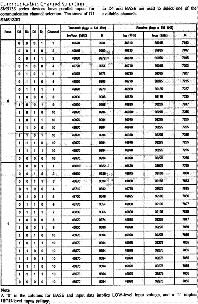
General
LDT is HIGH when the PLL is unlocked. LDT LDT goes LOW 6.4 ±0.4 ms after these conditions goes HIGH when the communication is no longer apply. See figure l . or when DOT has been HGH for 3.2 us.
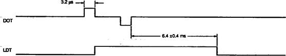
Figure l. Lock detector timing
F5K has an internal protective diode to prevent DOT and DOR have 3-state outputs and a.le electrostatic breakdown. The voltage at this pin intended for use with passive lowpass filters. must not exceed VDO. F5K should be left open when not in use.
 |
SM5133E
|
Base |
DI |
02 |
03 |
TranstTit (fREF = 5.0 Wiz) Channel |
|
|||||
|
fTWfE0 |
fRX |
fvco |
||||||||
|
O |
O |
1 |
496m |
46610 |
35915 |
7183 |
||||
|
o |
1 |
o |
49845 |
7187 |
||||||
|
o |
1 |
9972 |
46670 |
35975 |
||||||
|
1 |
O |
O |
497m |
46710 |
||||||
|
1 |
1 |
49875 |
9975 |
46730 |
7207 |
|||||
|
467m |
36075 |
7215 |
||||||||
|
$135 |
7227 |
|||||||||
|
1 |
468Ñ |
36175 |
||||||||
|
1 |
0 1 0 |
1 |
7247 |
|||||||
|
1 |
1 |
o |
10 |
49970 |
46970 |
|||||
|
11 |
46510 |
35815 |
||||||||
|
49710 |
9942 |
|||||||||
|
49740 |
465m |
35875 |
||||||||
|
49755 |
|
|||||||||
|
o |
O |
O |
O |
15 |
||||||
|
o |
o |
1 |
46610 |
49670 |
||||||
|
1 |
39150 |
|||||||||
|
o |
0 1 1 |
466m |
49860 |
39165 |
||||||
|
1 |
O |
O |
46710 |
gu2 |
49m |
39075 |
||||
|
1 |
1 |
49875 |
39180 |
|||||||
|
1 |
0 1 |
467Ñ |
49830 |
7827 |
||||||
|
7 1 |
4900 |
39195 |
||||||||
|
1 |
o |
o |
o |
9374 |
49930 |
7847 |
||||
|
1 |
||||||||||
|
1 |
1 |
o |
10 |
4œ70 |
499m |
39275 |
||||
|
1 |
1 |
11 |
46510 |
|||||||
|
1 |
O |
O |
12 |
49710 |
39015 |
|||||
|
|
1 |
13 |
9310 |
49725 |
||||||
|
14 |
46570 |
9314 |
49740 |
|||||||
|
l þ l |
15 |
9318 |
49755 |
|||||||
|
o l |
15 |
3318 |
49755 |
|||||||
Note
A '0' in the columns for BASE and input data implies LOW-Ievel input voltage, and a 'l' implies HIGH-Ievel input voltage.
CIRWfTS
TYPICAL APPLICATIONS
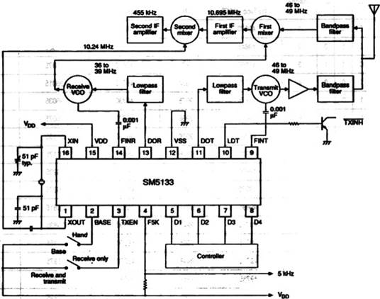
A with f 10.24 MHz, = 20 arxl CL = 30 PF is recommended.
Уважаемый посетитель!
Чтобы распечатать файл, скачайте его (в формате Word).
Ссылка на скачивание - внизу страницы.