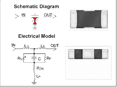
AVX has combined the best electrical characteristics of its TransGuard Transient Voltage Suppressors (TVS) and its Feedthru Capacitors into a single chip for state-of-the-art overvoltage circuit protection and EMI reduction over a broad range of frequencies. This unique combination of multilayer ceramic construction in a feedthru configuration gives the circuit designer a single 0805 chip that responds to transient events faster than any TVS device on the market today, and provides significant EMI attenuation when in the off-state.
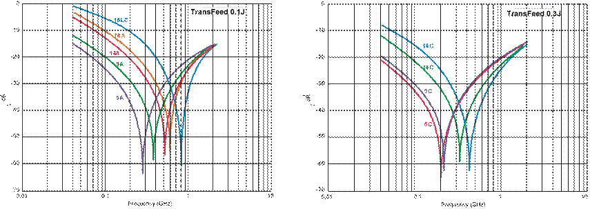
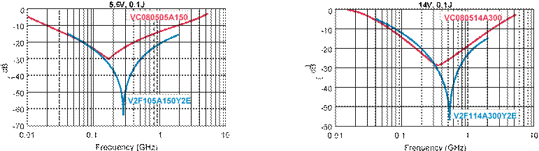
The reduction in parallel inductance, typical of the feedthru chip construction when compared to the construction of standard TVS or ceramic capacitor chips, gives the TransFeed product two very important electrical advantages: (1) faster “turn-on” time. Calculated response times of <200 pSec are not unusual with this device, and measured response times range from 200 – 250 pSec. The TransFeed “turn-on” characteristic is less than half that of an equivalent TransGuard part — and TransGuards clamp transient voltages faster than any other bipolar TVS solution such as diodes; (2) the second electrical advantage of lower parallel inductance, coupled with optimal series inductance, is the enhanced attenuation characteristics of the TransFeed product. Not only is there significantly greater attenuation at a higher self-resonance frequency, but the roll-off characteristic becomes much flatter, resulting in EMI filtering over a much broader frequency spectrum. Typical applications include filtering/protection on Microcontroller I/O Lines, Interface I/O Lines, Power Line Conditioning and Power Regulation.
• Fingerprint ID Circuit
• Magnetic Field Circuit
• LCD Dashboard Driver
Where designers are concerned with both transient voltage protection and EMI attenuation, either due to the electrical performance of their circuits or due to required compliance to specific EMC regulations, the TransFeed product is an ideal choice.
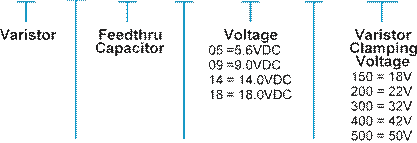
V 2 F 1 05 A 150
|
Chip Size 2 = 0805 3 = 0612 |
No. of Elements |
Energy Rating X = 0.05J |
A = 0.1J C = 0.3J
Y 2 E D P
![]()
![]()
![]()
![]()
![]() DCPackaging
DCPackaging
ResistanceCode
1 = 0.150 OhmsPcs./Reel
2 = 0.200 OhmsD = 1,000 3 = 0.250 OhmsR = 4,000
T = 10,000
|
Capacitance Tolerance Y = +100/-50% |
Feedthru Current D = 500 mA E = 750 mA F = 1.0 Amp |
Termination Finish P = Ni/Sn Alloy (Plated) M = Ni/Sn Pb (Plated) |
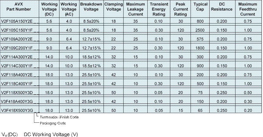
AVX Multilayer Ceramic Transient Voltage Suppressors
TVS Protection and EMI Attenuation in a Single Chip
 |
|
VW (AC) |
AC Working Voltage (V) |
|
VB |
Typical Breakdown Voltage (V @ 1mADC) |
|
VB Tol |
VB Tolerance is ± from Typical Value |
|
VC |
Clamping Voltage (V @ 1A 8x20µS) |
|
IL |
Maximum Leakage Current at the Working Voltage (µA) |
|
ET |
Transient Energy Rating (J, 10x1000µS) |
|
IP |
Peak Current Rating (A, 8x20µS) |
|
Cap |
Typical Capacitance (pF) @ 1MHz and 0.5 V |
|
DCR |
DC Resistance (Ohms) |
|
IFT |
Maximum Feedthru Current (A) |
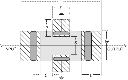
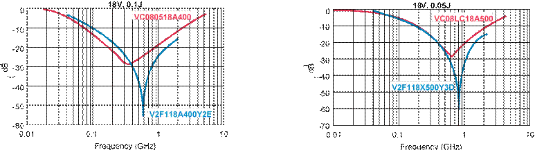
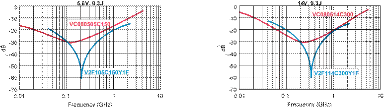
dB Attenuation vs Frequency
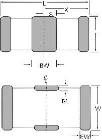
DIMENSIONS mm (inches)
|
L |
W |
T |
BW |
BL |
EW |
X |
S |
|
|
0805 |
2.01 ± 0.20 (0.079 ± 0.008) |
1.25 ± 0.20 (0.049 ± 0.008) |
1.143 Max. (0.045 Max.) |
0.46 ± 0.10 (0.018 ± 0.004) |
0.18 + 0.25 -0.08 (0.007 + 0.010 -0.003) |
0.25 ± 0.13 (0.010 ± 0.005) |
1.02 ± 0.10 (0.040 ± 0.004) |
0.23 ± 0.05 (0.009 ± 0.002) |
|
T |
P |
S |
W |
L |
C |
|
|
0805 |
3.45 (0.136) |
0.51 (0.020) |
0.76 (0.030) |
1.27 (0.050) |
1.02 (0.040) |
0.46 (0.018) |
TVS Protection and EMI Attenuation in a 4-Element Array
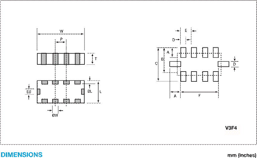
|
L |
W |
T |
BW |
BL |
ES |
P |
|||||||
|
1.60 ± 0.20 (0.063 ± 0.008) |
3.25 ± 0.15 (0.128 ± 0.006) |
1.22 Max. (0.048 Max.) |
0.41 ± 0.10 (0.016 ± 0.004) |
0.18 +0.25 -0.08 (0.007 +0.010 -0.003) |
0.41 ± 0.10 (0.016 ± 0.004) |
0.76 REF (0.030 REF) |
|||||||
|
mm (inches) |
|||||||||||||
|
A |
B |
C |
D |
E |
F |
||||||||
|
0.60 (0.024) |
1.60 (0.064) |
2.20 (0.088) |
0.35 (0.014) |
0.76 (0.030) |
2.60 (0.104) |
||||||||
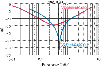 |
0805 – dB vs Frequency
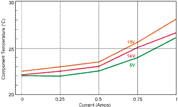 |
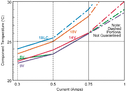
CURRENT vs TEMPERATURE
0805 – 0.3 Joule
AVX Multilayer Feedthru Varistors (MLVF) are an ideal choice The electrical model for a ZnO MLV and a ZnO Feedthru MLV for system designers with transient strike and broadband are shown below. The key difference in the model for
EMI/RFI concerns. the Feedthru is a transformation in parallel to series inducFeedthru Varistors utilize a ZnO varistor material and the tance. The added series inductance helps lower the injected electrode pattern of a feedthru capacitor. This combination transient peak current (by 2πfL) resulting in an additional benallows the package advantage of the feedthru and material efit of a lower clamping voltage. The lowered parallel inducadvantages of the ZnO dielectric to be optimized. tance decreases the turn on time for the varistor to <250ps
Уважаемый посетитель!
Чтобы распечатать файл, скачайте его (в формате Word).
Ссылка на скачивание - внизу страницы.