![]() CA3089
CA3089
November 1996 FM IF System
|
Features Description • For FM IF Amplifier Applications in High-Fidelity, Intersil CA3089 is a monolithic integrated circuit that proAutomotive, and Communications Receivers vides all the functions of a comprehensive FM-IF system. • Includes: IF Amplifier, Quadrature Detector, AF The block diagram shows the CA3089 features, which Preamplifier, and Specific Circuits for AGC, AFC, Muting include a three-stage FM-IF amplifier/limiter configuration (Squelch), and Tuning Meter with level detectors for each stage, a doubly-balanced quadrature FM detector and an audio amplifier that features • Exceptional Limiting Sensitivitythe optional use of a muting (squelch) circuit. at -3dB Point. . . . . . . . . . . . . . . . . . . . . . . . . . 12µV (Typ) • Low Distortion: The advanced circuit design of the IF system includes desir(with Double-Tuned Coil). . . . . . . . . . . . . . . . 0.1% (Typ) able deluxe features such as delayed AGC for the RF tuner, and AFC drive circuit, and an output signal to drive a tuning • Single-Coil Tuning Capability meter and/or provide stereo switching logic. In addition, inter• High Recovered Audio. . . . . . . . . . . . . . . . 400mV (Typ) nal power supply regulators maintain a nearly constant current drain over the voltage supply range of +8.5V to +16V. • Provides Specific Signal for Control of Interchannel Muting (Squelch) The CA3089 is ideal for high-fidelity operation. Distortion in a • Provides Specific Signal for Direct Drive of a Tuning CA3089 FM-IF System is primarily a function of the phase Meter linearity characteristic of the outboard detector coil. • Provides Delayed AGC Voltage for RF Amplifier • Provides a Specific Circuit for Flexible AFC • Internal Supply-Voltage Regulators Ordering Information
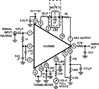
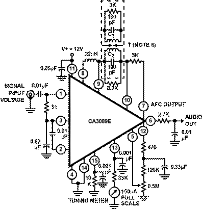
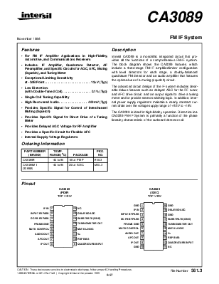
Pinout CA3089 CA3089 (PDIP) (SOIC) TOP VIEW TOP VIEW
IF IN 16 NC IF IN 19 DELAYED AGC INPUT BYPASS 15 DELAYED AGC INPUT BYPASS 18 GND DC FB BYPASS 14 SUBSTRATE (GND) DC FB BYPASS 17 SUBSTRATE (GND) FRAME GND 13 TUNING METER OUT FRAME GND 16 TUNING METER OUT MUTE CONTROL 12 MUTE LOGIC MUTE CONTROL 15 MUTE LOGIC AUDIO OUT 11 V+ AUDIO OUT 14 V+ AFC OUT 10 REF BIAS AFC OUT 13 REF BIAS IF OUT 12 IF OUT 9 QUADRATURE INPUTQUADRATURE INPUT GND 10 11 NC |
CAUTION: These devices are sensitive to electrostatic discharge; follow proper IC Handling Procedures. File Number 561.3
1-888-INTERSIL or 321-724-7143 | Copyright © Intersil Corporation 1999
|
Absolute Maximum Ratings |
Thermal Information |
|
Supply Voltage Between V+ and Frame GND . . . . . . . . . . . . . . . . . . . . . . . . . 16V Between V+ and Substrate GND . . . . . . . . . . . . . . . . . . . . . . 16V DC Current (Out of Delayed AGC) . . . . . . . . . . . . . . . . . . . . . . .2mA Operating Conditions Temperature Range . . . . . . . . . . . . . . . . . . . . . . . . . -40oC to 85oC |
Thermal Resistance (Typical, Note 1) θJA (oC/W) PDIP Package . . . . . . . . . . . . . . . . . . . . . . . . . . . . . 90 SOIC Package. . . . . . . . . . . . . . . . . . . . . . . . . . . . . 80 Maximum Junction Temperature (Plastic Package) . . . . . . . . 150oC Maximum Storage Temperature Range . . . . . . . . . -65oC to 150oC Maximum Lead Temperature (Soldering 10s). . . . . . . . . . . . 300oC |
(SOIC - Lead Tips Only)
CAUTION: Stresses above those listed in “Absolute Maximum Ratings” may cause permanent damage to the device. This is a stress only rating and operation of the device at these or any other conditions above those indicated in the operational sections of this specification is not implied.
NOTE:
1. θJA is measured with the component mounted on an evaluation PC board in free air.
![]()
Electrical Specifications V+ = 12V (See Figures 3 and 4)
|
(NOTE 3) PARAMETER |
TEST CONDITIONS |
TEMP. (oC) |
MIN |
TYP |
MAX |
UNITS |
||
|
DC CHARACTERISTICS |
||||||||
|
Quiescent Circuit Current |
No signal input, Non muted |
25 |
16 |
23 |
30 |
mA |
||
|
DC Voltages |
Terminal 1 (IF Input) |
25 |
1.2 |
1.9 |
2.4 |
V |
||
|
Terminal 2 (AC Return to Input) |
25 |
1.2 |
1.9 |
2.4 |
V |
|||
|
Terminal 3 (DC Bias to Input) |
25 |
1.2 |
1.9 |
2.4 |
V |
|||
|
Terminal 6 (Audio Output) |
25 |
5.0 |
5.6 |
6.0 |
V |
|||
|
Terminal 10 (DC Reference) |
25 |
5.0 |
5.6 |
6.0 |
V |
|||
|
DYNAMIC CHARACTERISTICS |
||||||||
|
Input Limiting Voltage (-3dB point), V1 (lim) |
- |
fO = 10.7MHz, fMOD = 400Hz, Deviation = ±75kHz |
25 |
- |
12 |
25 |
µV |
|
|
AM Rejection (Terminal 6), AMR |
VIN = 0.1V, AM Mod. = 30% |
25 |
45 |
55 |
- |
dB |
||
|
Recovered AF Voltage (Terminal 6) VO (AF) |
VIN = 0.1V |
25 |
300 |
400 |
500 |
mV |
||
|
Total Harmonic Distortion, THD (Note 2) |
Single Tuned (Terminal 6) |
25 |
- |
0.5 |
1.0 |
% |
||
|
Double Tuned (Terminal 6) |
25 |
- |
0.1 |
- |
% |
|||
|
Signal Plus Noise to Noise Ratio (Terminal 6) |
25 |
60 |
67 |
- |
dB |
|||
NOTES:
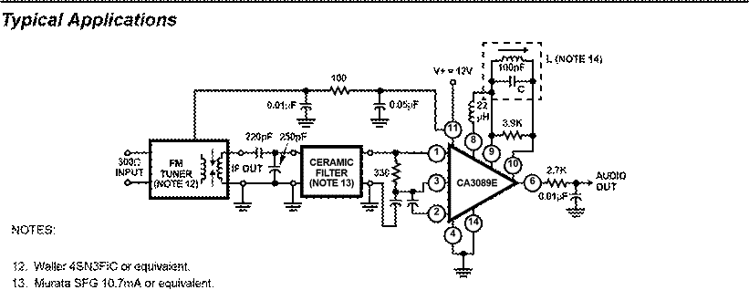
2. THD characteristics are essentially a function of the phase characteristics of the network connected between Terminals 8, 9, and 10.
3. Terminal numbers refer to 16 Lead PDIP.
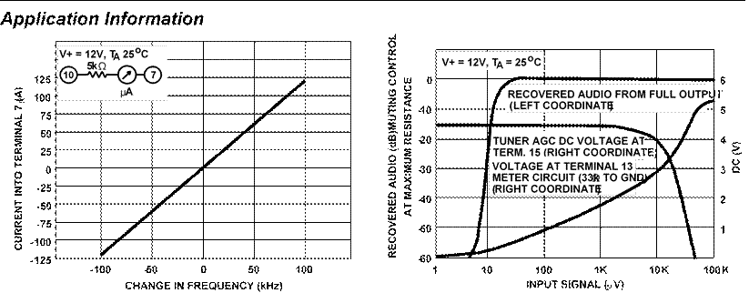
FIGURE 1. AFC CHARACTERISTICS (CURRENT AT TERMINAL FIGURE 2. MUTING ACTION, TUNER AGC, AND TUNING
7) vs CHANGE IN FREQUENCY. (SEE TEST CIRCUIT METER OUTPUT vs INPUT SIGNAL VOLTAGE. (SEE
FIGURE 3.) TEST CIRCUIT FIGURE 3.)
 µF
µF
NOTES:
4. All resistance values are in ohms.
5. L tunes with 100pF (C) at 10.7MHz.
6. Q0 (unloaded) ≅ 75 (G.I. Automatic Mfg. Div. EX22741 or equivalent).
NOTES:
7. All resistance values are in ohms.
8. T PRI. - Q0 (unloaded) ≅ 75 (tunes with 100pF (C1) 20↑ of 34e on 7/32” dia. form).
9. SEC. - Q0 (unloaded) ≅ 75 (tunes with 100pF (C2) 20↑ of 34e on 7/32” dia. form).
10. kQ (percent of critical coupling) ≅ 70%.
(Adjusted for coil voltage VC) = 150mV.
Above values permit proper operation of mute (squelch) circuit “E” type slugs, spacing 4mm.
 11. All resistance
values are in ohms.
11. All resistance
values are in ohms.
14. L tunes with 100pF (C) at 10.7MHz Q0 unloaded≅ 75 Performance Data at fO = 98MHz, fMOD = 400Hz
Уважаемый посетитель!
Чтобы распечатать файл, скачайте его (в формате Word).
Ссылка на скачивание - внизу страницы.

 GND 20
GND
GND 20
GND