Sep 1, 2005
A UV silicon detector contains a layer of silicon-rich silicon oxide; the layer absorbs UV and emits visible light that is sensed by the detector, raising sensitivity by a factor of ten.
DAINET BERMAN-MENDOZA, MARIANO ACEVES-MIJARES, LUIS RAÚL BERRIEL-VALDOS, JAZMÍN CARRANZA, JORGE PEDRAZA, CARLOS DOMÍNGUEZ-HORNA, AND CIRO FALCONY
Since the discovery of photoluminescence in silicon (Si) nanocrystals embedded in silicon dioxide, much effort has been expended to take advantage of this emission. Many techniques have been used to obtain Si nanocrystals. Chemical-vapor deposition (CVD), however, is a simple way to obtain silicon-rich silicon oxide (SRO) films. This material is normally modeled as silicon dioxide that contains Si nanocrystals. It has been shown that SRO films obtained by low-pressure CVD (LPCVD) radiate intensely when they are illuminated by UV energy.1 The SRO emissions match the wavelength range in which Si is very sensitive (see Fig. 1).
|
Click here to enlarge image
|
The large number of potential applications has lead to great interest in developing UV Si sensors because the technology is mature and cheaper than others; however, crystalline Si photodiodes exhibit a low efficiency in the UV region (200 to 400 nm). To remedy this problem, the high sensitivity of Si in the visible can be extended to the UV region by integrating a silicon detector with an SRO film. We have developed a UV silicon detector (patent pending) made of Si and SRO that shows high efficiency and is completely compatible with silicon fabrication technology.
|
Click here to enlarge image
|
When irradiated with UV light, the SRO film in the detector emits IR and visible light that is absorbed by the p-n silicon photodetector, which generates a photocurrent proportional to the UV radiation (see Fig. 2). The main limitation of p-n photodiodes is the dark current, which defines the minimum energy detectable by the diode. In our device, a guard ring is implemented to decrease the dark current. This ring allows the reverse-polarization voltage to be increased, maintaining a low leakage current.2
Silicon-rich oxide is a material that shows great potential for carrying out optoelectronic functions in Si integrated circuits.3 This material can be fabricated using several technological processes: Si-implanted thermal oxide, LPCVD, and plasma-enhanced chemical-vapor deposition. In general, the substrate material is Si.
In the LPCVD process, the Si excess in the SRO film is controlled by adjusting the flow-rate ratio (Ro), which is the ratio of the quantities of nitrous oxide and silane, the reactive gases used during the growth of the film. This method produces films with diverse Si excesses; values of Ro between 10 and 30 generate Si excess in the SRO between 10% and 6%, respectively.3
After annealing at high temperatures, the SRO acquires excellent optoelectronic properties. These properties appear as a consequence of diverse effects, including consolidation and size change of Si nanocrystals, among others.
The substrates consisted of p-type, 10‑µm epitaxial Si wafers with a resistivity of 8 ohms-cm. After cleaning, an oxide film was grown to define a diffusion region. The oxide was etched and standard phosphorous diffusion used to form the p-n junction; the SRO was deposited over this structure. A phosphosilicate-glass film was then deposited and annealed in water and nitrogen for 30 minutes, after which aluminum contacts were etched and patterned. Finally, the devices were mounted on integrated-circuit frames.
The UV sensor was characterized with a spectrophotometer that measured over a 190- to 900-nm wavelength range using deuterium and tungsten bromide lamps. The current was measured with an electrometer. With the same setup, UV-enhanced commercial p-n diodes were measured as a comparison and to determine the source optical power.
|
Click here to enlarge image
|
Уважаемый посетитель!
Чтобы распечатать файл, скачайте его (в формате Word).
Ссылка на скачивание - внизу страницы.
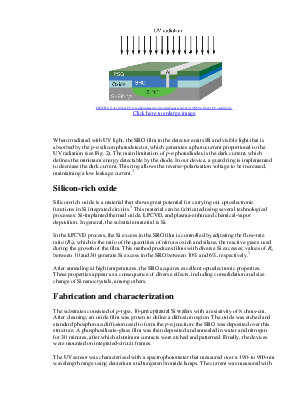
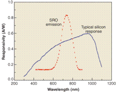 FIGURE 1. Photoemission
wavelengths of a silicon-rich silicon oxide film (which absorbs UV radiation
and emits in the visible) fall close to the peak spectral response of
silicon.
FIGURE 1. Photoemission
wavelengths of a silicon-rich silicon oxide film (which absorbs UV radiation
and emits in the visible) fall close to the peak spectral response of
silicon. 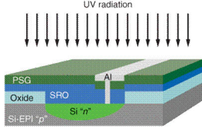 FIGURE 2. A silicon UV p-n
photodetector incorporates a layer of SRO to boost UV sensitivity.
FIGURE 2. A silicon UV p-n
photodetector incorporates a layer of SRO to boost UV sensitivity. 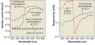 FIGURE 3. An SRO silicon
sensor shows an order-of-magnitude increase in density current (left) and
responsivity (right) in the UV.
FIGURE 3. An SRO silicon
sensor shows an order-of-magnitude increase in density current (left) and
responsivity (right) in the UV.