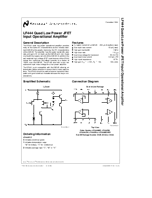
National Semiconductor Corporation TL/H/9156 RRD-B30M115/Printed in U. S. A.
|
Absolute Maximum Ratings If Military/Aerospace specified devices are required, please contact the National Semiconductor Sales Office/Distributors for availability and specifications. LF444A LF444 Supply Voltage g22V g18V Differential Input Voltage g38V g30V Input Voltage Range g19V g15V (Note 1) Output Short Circuit Continuous Continuous Duration (Note 2) D Package N, M Packages Power Dissipation 900 mW 670 mW (Notes 3 and 9) Tj max 150§C 115§C ijA (Typical) 100§C/W 85§C/W |
LF444A/LF444 Operating Temperature Range (Note 4) Storage Temperature Range b65§C s TA s 150§C ESD Tolerance (Note 10) Rating to be determined Soldering Information Dual-In-Line Packages (Soldering, 10 sec.) 260§C Small Outline Package Vapor Phase (60 sec.) 215§C Infrared (15 sec.) 220§C See AN-450 ‘‘Surface Mounting Methods and Their Effect on Product Reliability’’ for other methods of soldering surface mount devices. |
|||||||||
|
DC Electrical Characteristics (Note 5) |
||||||||||
|
Symbol |
Parameter |
Conditions |
LF444A |
LF444 |
Units |
|||||
|
Min |
Typ |
Max |
Min |
Typ |
Max |
|||||
|
VOS |
Input Offset Voltage |
RS e 10k, TA e 25§C |
2 |
5 |
3 |
10 |
mV |
|||
|
0§C s TA sa70§C |
6.5 |
12 |
mV |
|||||||
|
b55§C s TA sa125§C |
8 |
mV |
||||||||
|
DVOS/DT |
Average TC of Input Offset Voltage |
RS e 10 kX |
10 |
10 |
mV/§C |
|||||
|
IOS |
Input Offset Current |
VS eg15V (Notes 5, 6) |
Tj e 25§C |
5 |
25 |
5 |
50 |
pA |
||
|
Tj e 70§C |
1.5 |
1.5 |
nA |
|||||||
|
Tj e 125§C |
10 |
nA |
||||||||
|
IB |
Input Bias Current |
VS eg15V (Notes 5, 6) |
Tj e 25§C |
10 |
50 |
10 |
100 |
pA |
||
|
Tj e 70§C |
3 |
3 |
nA |
|||||||
|
Tj e 125§C |
20 |
nA |
||||||||
|
RIN |
Input Resistance |
Tj e 25§C |
1012 |
1012 |
X |
|||||
|
AVOL |
Large Signal Voltage Gain |
VS eg15V, VO eg10V RL e 10 kX, TA e 25§C |
50 |
100 |
25 |
100 |
V/mV |
|||
|
Over Temperature |
25 |
15 |
V/mV |
|||||||
|
VO |
Output Voltage Swing |
VS eg15V, RL e 10 kX |
g12 |
g13 |
g12 |
g13 |
V |
|||
|
VCM |
Input Common-Mode |
g16 |
a18 |
g11 |
a14 |
V |
||||
|
Voltage Range |
b17 |
b12 |
V |
|||||||
|
CMRR |
Common-Mode Rejection Ratio |
RS s 10 kX |
80 |
100 |
70 |
95 |
dB |
|||
|
PSRR |
Supply Voltage Rejection Ratio |
(Note 7) |
80 |
100 |
70 |
90 |
dB |
|||
|
IS |
Supply Current |
0.6 |
0.8 |
0.6 |
1.0 |
mA |
||||
|
AC Electrical Characteristics (Note 5) |
||||||||||
|
Symbol |
Parameter |
Conditions |
LF444A |
LF444 |
Units |
|||||
|
Min |
Typ |
Max |
Min |
Typ |
Max |
|||||
|
Amplifier-to-Amplifier Coupling |
b120 |
b120 |
dB |
|||||||
|
SR |
Slew Rate |
VS e |
g15V, TA e 25§C |
1 |
1 |
V/ms |
||||
|
GBW |
Gain-Bandwidth Product |
VS e |
g15V, TA e 25§C |
1 |
1 |
MHz |
||||
|
en |
Equivalent Input Noise Voltage |
TA e 25§C, RS e 100X, |
35 |
35 |
nV/0Hz |
|||||
|
f e 1 kHz |
||||||||||
|
in |
Equivalent Input Noise Current |
TA e 25§C, f e 1 kHz |
0.01 |
0.01 |
pA/0Hz |
|||||
|
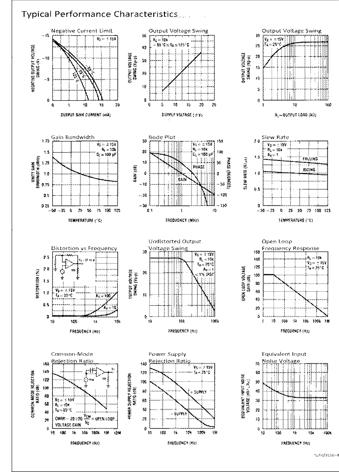
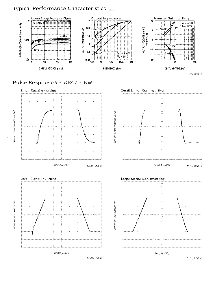
Note 1: Unless otherwise specified the absolute maximum negative input voltage is equal to the negative power supply voltage. Note 2: Any of the amplifier outputs can be shorted to ground indefinitely, however, more than one should not be simultaneously shorted as the maximum junction temperature will be exceeded. Note 3: For operating at elevated temperature, these devices must be derated based on a thermal resistance of ijA. Note 4: The LF444A is available in both the commercial temperature range 0§C s TA s 70§C and the military temperature range b55§C s TA s 125§C. The LF444 is available in the commercial temperature range only. The temperature range is designated by the position just before the package type in the device number. A ‘‘C’’ indicates the commercial temperature range and an ‘‘M’’ indicates the military temperature range. The military temperature range is available in ‘‘D’’ package only. Note 5: Unless otherwise specified the specifications apply over the full temperature range and for VS eg20V for the LF444A and for VS eg15V for the LF444. VOS, IB, and IOS are measured at VCM e 0. Note 6: The input bias currents are junction leakage currents which approximately double for every 10§C increase in the junction temperature, Tj. Due to limited production test time, the input bias currents measured are correlated to junction temperature. In normal operation the junction temperature rises above the ambient temperature as a result of internal power dissipation, PD. Tj e TA a ijAPD where ijA is the thermal resistance from junction to ambient. Use of a heat sink is recommended if input bias current is to be kept to a minimum. Note 7: Supply voltage rejection ratio is measured for both supply magnitudes increasing or decreasing simultaneously in accordance with common practice from g15V to g5V for the LF444 and from g20V to g5V for the LF444A. Note 8: Refer to RETS444X for LF444MD military specifications. Note 9: Max. Power Dissipation is defined by the package characteristics. Operating the part near the Max. Power Dissipation may cause the part to operate outside guaranteed limits. Note 10: Human body model, 1.5 kX in series with 100 pF. Typical Performance Characteristics
TL/H/9156–3 |
||||||||||
|
Application Hints This device is a quad low power op amp with JFET input The amplifiers will drive a 10 kX load resistance to g10V devices (BI-FETTM). These JFETs have large reverse break- over the full temperature range. If the amplifier is forced to down voltages from gate to source and drain eliminating the drive heavier load currents, however, an increase in input need for clamps across the inputs. Therefore, large differen- offset voltage may occur on the negative voltage swing and tial input voltages can easily be accommodated without a finally reach an active current limit on both positive and neglarge increase in input current. The maximum differential in- ative swings. put voltage is independent of the supply voltages. However, Precautions should be taken to ensure that the power supneither of the input voltages should be allowed to exceed ply for the integrated circuit never becomes reversed in pothe negative supply as this will cause large currents to flow larity or that the unit is not inadvertently installed backwards which can result in a destroyed unit. in a socket as an unlimited current surge through the resultExceeding the negative common-mode limit on either input ing forward diode within the IC could cause fusing of the will force the output to a high state, potentially causing a internal conductors and result in a destroyed unit. reversal of phase to the output. Exceeding the negative As with most amplifiers, care should be taken with lead common-mode limit on both inputs will force the amplifier dress, component placement and supply decoupling in oroutput to a high state. In neither case does a latch occur der to ensure stability. For example, resistors from the outsince raising the input back within the common-mode range put to an input should be placed with the body close to the again puts the input stage and thus the amplifier in a normal input to minimize ‘‘pick-up’’ and maximize the frequency of operating mode. the feedback pole by minimizing the capacitance from the Exceeding the positive common-mode limit on a single input input |
Уважаемый посетитель!
Чтобы распечатать файл, скачайте его (в формате Word).
Ссылка на скачивание - внизу страницы.
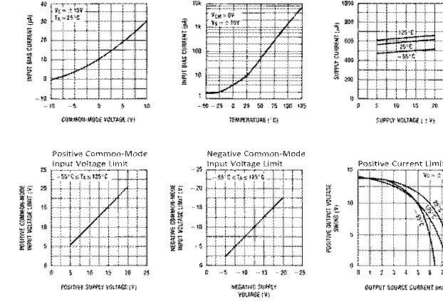 Input Bias Current Input
Bias Current Supply Current
Input Bias Current Input
Bias Current Supply Current