a Digitally Controlled VGA
![]() LF to
700MHz Preliminary Technical Data AD8370
LF to
700MHz Preliminary Technical Data AD8370
Differential Input and Output
200Ω Differential Input
100Ω Differential Output
7dB Noise Figure @ Maximum Gain
Two Tone IP3 of 31dBm @ 70MHz
-3dB Bandwidth of 700MHz
40dB Precision Gain Range
Serial 7-bit Interface
Pin Programmable Low and High Gain Low Range -11 to 17dB
High Range 6 to 34dB Wide Input Dynamic Range
Operation Down to a 3 V Supply
Power Down Feature
APPLICATIONS
Differential ADC Driver IF Sampling Receivers
Cellular/PCS Base Stations RF/IF Gain Stages
SAW Filter Interfacing
Single-Ended to Differential Conversion
The AD8370 is a low cost, digitally controlled, variable gain amplifier that provides both high IP3 and low noise figure. The excellent distortion performance and wide bandwidth makes the AD8370 a suitable gain control device for modern receiver designs.
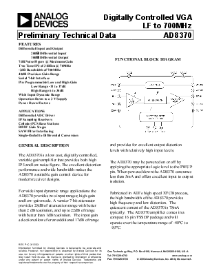
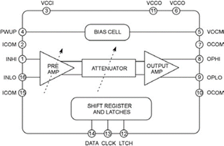
For wide input dynamic range applications the AD8370 provides two input ranges; high-gain and low-gain mode. A vernier 7-bit attenuator provides 28dB of attenuation range with better than 2 dB resolution, and up to 22dB of range with better than 1dB resolution. The input gain selection allows for an additional 17dB of range FUNCTIONAL BLOCK DIAGRAM
and provides for excellent output distortion levels with relatively high input levels.
The AD8370 may be powered on or off by applying the appropriate logic level to the PWUP pin. When powered down the AD8370 consumes less than 5mA and offers excellent input to output isolation.
|
REV. PrC 3/12/03 |
Fabricated in ADI’s high speed XFCB process, the high bandwidth of the AD8370 provides high frequency and low distortion. The quiescent current of the AD8370 is 78mA typically. The AD8370 amplifier comes in a compact 16 pin TSSOP package and will operate over the temperature range of -40°C to +85°C.
Information furnished by Analog Devices is believed to be accurate and reliable. However, no responsibility is assumed by Analog Devices for its use, nor for any infringements of patents or other rights of third parties that may result from its use. No license is granted by implication or otherwise under any patent or patent rights of Analog Devices. Trademarks and registered trademarks are the property of their respective companies.
One Technology Way, P.O. Box 9106, Norwood, MA 02062-9106, U.S.A.
Tel: 781/329-4700 www.analog.com Fax: 781/326-8703 © 2003 Analog Devices, Inc. All rights reserved.
AD8370-SPECIFICATIONS (VS=5V, T=25°C, RS=200Ω, RL = 100Ω at max gain unless otherwise noted)
|
Parameter |
Conditions |
Min |
Typ |
Max |
Units |
|
DYNAMIC PERFORMANCE - 3 dB Bandwidth |
Vout<1 Vp-p |
700 |
MHz |
||
|
Bandwidth for 0.1 dB Flatness |
Vout<1 Vp-p |
TBD |
MHz |
||
|
INPUT STAGE Maximum Input |
Low Gain (1dB Compression) |
1.13 |
Vrms |
||
|
Maximum Input |
High Gain (1dB Compression) |
500 |
mVrms |
||
|
Input Resistance |
Differential, f=10MHz |
200 |
Ω |
||
|
Input Capacitance |
Differential, f=10MHz |
TBD |
pF |
||
|
Common Mode Input Range |
3.2 |
Vp-p |
|||
|
CMRR |
Differential, f=10MHz |
60 |
dB |
||
|
GAIN CONTROL INTERFACE (GAIN) High Gain |
Gain Code = 127 |
34.1 |
dB |
||
|
High Gain |
Gain Code = 5 |
6.0 |
dB |
||
|
Low Gain |
Gain Code = 127 |
17.1 |
dB |
||
|
Low Gain |
Gain Code = 5 |
-11.0 |
dB |
||
|
Step Response |
For 6 dB Gain Step |
10 |
TBD |
ns |
|
|
OUTPUT STAGE Output Voltage Swing |
RL ≥ 1kΩ (1dB Compression) |
8.4 |
Vp-p |
||
|
Output Resistance |
Differential, f=10MHz |
100 |
Ω |
||
|
Output Capacitance |
Differential, f=10MHz |
TBD |
pF |
||
|
NOISE/HARMONIC PERFORMANCE 10MHz Noise Figure |
7.2 |
dB |
|||
|
2nd Harmonic |
Vout = 1Vp-p, RL = 100Ω |
-75 |
dBc |
||
|
3rd Harmonic |
Vout = 1Vp-p, RL = 100Ω |
-71 |
dBc |
||
|
Two-Tone IMD |
1Vp-p Composite |
-72 |
dBc |
||
|
Output 1dB Compression Point |
15.8 |
dBm |
|||
|
70MHz Noise Figure |
7.4 |
dB |
|||
|
2nd Harmonic |
Vout = 1Vp-p, RL = 100Ω |
-68 |
dBc |
||
|
3rd Harmonic |
Vout = 1Vp-p, RL = 100Ω |
-61 |
dBc |
||
|
Two-Tone IMD |
1Vp-p Composite |
-72 |
dBc |
||
|
Output 1dB Compression Point |
15.8 |
dBm |
|||
|
140MHz Noise Figure |
7.6 |
dB |
|||
|
2nd Harmonic |
Vout = 1Vp-p, RL = 100Ω |
-64 |
dBc |
||
|
3rd Harmonic |
Vout = 1Vp-p, RL = 100Ω |
-52 |
dBc |
||
|
Two-Tone IMD |
1Vp-p Composite |
-69 |
dBc |
||
|
Output 1dB Compression Point |
14.8 |
dBm |
AD8370-SPECIFICATIONS (VS=5V, T=25°C, RS=200Ω, RL = 100Ω at max gain unless otherwise noted)
|
Parameter |
Conditions |
Min |
Typ |
Max |
Units |
|
NOISE/HARMONIC PERFORMANCE 190MHz Noise Figure |
7.6 |
dB |
|||
|
2nd Harmonic |
Vout = 1Vp-p, RL = 100Ω |
-62 |
dBc |
||
|
3rd Harmonic |
Vout = 1Vp-p, RL = 100Ω |
-47 |
dBc |
||
|
Two-Tone IMD |
1Vp-p Composite |
-67 |
dBc |
||
|
Output 1dB Compression Point |
13.6 |
dBm |
|||
|
240MHz Noise Figure |
7.7 |
dB |
|||
|
2nd Harmonic |
Vout = 1Vp-p, RL = 100Ω |
TBD |
dBc |
||
|
3rd Harmonic |
Vout = 1Vp-p, RL = 100Ω |
TBD |
dBc |
||
|
Two-Tone IMD |
1Vp-p Composite |
-65 |
dBc |
||
|
Output 1dB Compression Point |
13.5 |
dBm |
|||
|
380MHz Noise Figure |
7.8 |
dB |
|||
|
2nd Harmonic |
Vout = 1Vp-p, RL = 100Ω |
TBD |
dBc |
||
|
3rd Harmonic |
Vout = 1Vp-p, RL = 100Ω |
TBD |
dBc |
||
|
Two-Tone IMD |
1Vp-p Composite |
-56 |
dBc |
||
|
Output 1dB Compression Point |
11.2 |
dBm |
|||
|
POWER INTERFACE Supply Voltage |
2.7 |
5.5 |
V |
||
|
Quiescent Current |
PWUP high |
78 |
mA |
||
|
vs. Temperature |
-40°C ≤ TA ≤ 85°C |
TBD |
TBD |
mA |
|
|
Total Supply Current |
PWUP high, Vout = 1Vp-p, RL= 100 Ω (includes load current) |
80 |
mA |
||
|
Power Down Current |
PWUP low |
4 |
mA |
||
|
vs. Temperature |
-40°C ≤ TA ≤ 85°C |
TBD |
TBD |
mA |
|
|
POWER DOWN INTERFACE Power Up Threshold |
1.2 |
V |
|||
|
PWUP Input Bias Current |
PWUP = 0 V |
135 |
nA |
Notes
Typical Performance Characteristics (VS = 5V, RS=200Ω, RL=100Ω, T=25°C, unless otherwise noted)
|
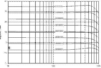
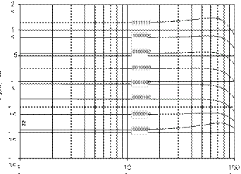
TPC 1. High-Gain Mode AC Response |
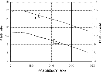
TPC 4. Output Third Order Intercept versus Frequency at Maximum Gain |
 Frequency
- MHz
Frequency
- MHz 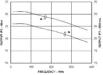
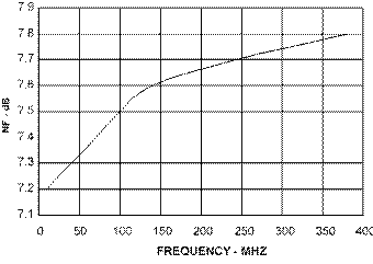
Frequency - MHz
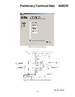
Basic Connections Figure 1 shows the minimum connections required for basic operation of the AD8370. Supply voltages between 2.7 and 5.5V are allowed. The supply to the VCCO and VCCI pins should be decoupled with at least one low inductance surface-mount ceramic capacitor of 0.1 µF placed as close as possible to the device. More effective decoupling is provided by placing a 100pF capacitor in parallel and including a ferrite bead in series with the supply.
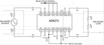 |
performance when used in an unbalanced environment.
|
gain adjustment. The linear voltage gain can be expressed with respect to the gain code as: A = GainCode Vernier⋅ ⋅(1 (+ PreGain −1)⋅MSB) where Av is the linear voltage gain. |
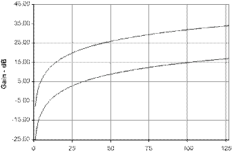
The AD8370 is designed to be a fine gain adjustment variable gain amplifier. The gain control transfer function is linear in voltage gain. On a decibel scale, this results in the exponential transfer functions indicated in TPC 3. At the low end of the gain transfer function, the slope is steep, providing a rather coarse control function. At the higher end of the gain control range the dB step size is decreased allowing for precise
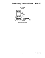
The AD8370 is designed to be used in differential signal chains. Differential signaling allows for improved evenorder harmonic cancellation and better common-mode immunity than can be achieved using a single-ended design. In order to fully exploit these benefits, it is necessary to drive
Уважаемый посетитель!
Чтобы распечатать файл, скачайте его (в формате Word).
Ссылка на скачивание - внизу страницы.