The purpose of this paper is to provide a detailed description of the Dupline Fieldbus operating principles.
There are 4 basic components in a Dupline network:
This unit generates the carrier square-wave signal that enables the communication on the bus. On a Dupline network, there is always one, and only one, channel generator installed. Some Channel Generators have built-in intelligent functions and serial interfacing capabilities as well
The transmitters are the devices that feed information into the bus. Typical examples are input modules for digital and analog signals. Some transmitters are powered from the bus signal.
The receivers are output devices that controls the outputs according to the information received from the bus. Typical examples are relay output modules and analog output modules.
The Dupline bus uses a 2-wire cable for the communication. No special cable is required, so it is not necessary to use shielded or twisted cable. The cable topology is free.
THE DUPLINE MULTIPLEXING PRINCIPLE
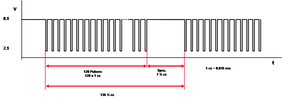
Dupline is based on a simple and well-proven hardware-oriented time-division multiplexing principle that provides a much more compact and straightforward transmission of a few bits from each node than the traditional message-oriented method. The Channel Generator generates a square-wave voltage signal consisting of a synchronization pulse with a length of 7 ½ clock cycles (cc) followed by 128 pulses each with a length of 1 cc and starting with a negative going transition. The basic frequency of the Dupline signal is 1024 Hz, so one cc = 976ms.
This ”pulse train” is repeated continuously. The voltage levels and the timing of the signal are shown in the diagram below.

Each digital input or output on the bus needs to have one of the 128 bit-addresses in the system assigned to it. An address is in fact a definition of the pulse number the I/O shall use for transmitting or receiving its signal. In practice, the address assignment is done by means of a simple handheld coding device that downloads the selected addresses to the Dupline ASIC communication chip, which is the central electronic component in each Dupline module. A node on the bus can have between 1 and 8 digital I/Os, but due to the individual addressing of I/Os it is only the ones which have been assigned an address that occupy transmission capacity.
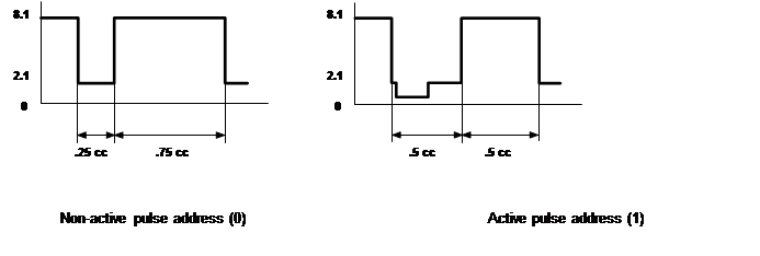
The ASIC communication chip has a built-in pulse-counter that increments by one for every negative going transition and which is reset when a synchronization pulse is detected. Every time a new pulse arrives, the ASIC compares the addresses (pulse numbers), which have been assigned to its individual I/O-pins with the actual pulse number on the bus. If there is an address match for an activated input, the ASIC transmits a signal on the bus by pulling down the voltage level from 2.2 V to app. 0.7 V by means of an open collector transistor. The pull-down is done immediately after the pulse has started and is detected by the Channel Generator, which in turn keys the information into the pulse by changing the width of the low period from 0.25 cc to 0.5 cc. The ASIC’s on the bus, which have outputs matching the actual pulse address, measure the width of the low period and update the state of the output accordingly. Thereby a peer-to-peer transfer of an input signal at one location to an output signal at another location has taken place.
The difference between a non-active (0) and active (1) pulse address is shown in the diagram below. Note the pull-down of the voltage level from 2.1 V to app. 0.7 V on the active address and the resulting change of the width of the low period from 0.25 cc to 0.75 cc.
 |
One of the means the receivers use to verify data integrity is that they do not change the state of an output until the opposite signal has been received in two consecutive pulse-trains. As a result the worst-case response time from input to output is 2 x 136 cc = 272 cc.
ASIC OPERATION
An RC low-pass filter with a cut-off frequency of 16 KHz directly on the ASIC’s Dupline input removes high frequency noise (see attached transmitter diagram in appendix A). After that, internally in the ASIC, The Dupline input signal goes to a voltage comparator with hysteresis. The High-to-low trigger level is app. 3.2 V and the Low-to-high trigger level is app. 3.8 V.
The ASIC chip samples the Dupline signal on the output of the comparator with a rate of app. 32 kHz, in other words app 30 ms between each sample. This means 32 samples per Dupline pulse. After that, the signal goes into a de-bounce filter and a couple of other digital filters to suppress false triggers and level detections. Detection of signal transitions and levels are never based on single samples.
In the transmitter diagram in appendix A, please note T9. This is the open collector transistor used to pull down the voltage level from 2.1 VDC to 0.7 VDC when the transmitter needs to send an active signal. Note also that this transmitter is powered from the bus signal.
The ASIC monitors the signal line for 2 s before becoming operational on the bus. It monitors the timing and level of the signal constantly and in case of a faulty condition, the ASIC “goes off-line” and brings the outputs to a user pre-defined state.
CHANNEL GENERATOR OPERATION
Уважаемый посетитель!
Чтобы распечатать файл, скачайте его (в формате Word).
Ссылка на скачивание - внизу страницы.