 S E M I
C O N D U C T O R HGTB12N60D1C
S E M I
C O N D U C T O R HGTB12N60D1C
April 1995 12A, 600V Current Sensing N-Channel IGBT
• rDS(ON). . . . . . . . . . . . . . . . . . . . . . . . . . . . . . . . . . . . . . . . . . . . . . . . 0.27Ω 54 32
• Low VCE(SAT) at 25A . . . . . . . . . . . . . . . . . . . . . . . . . . . . . . . . 2.5V (Typ) 1
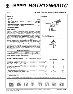
• Ultra-Fast Turn-On . . . . . . . . . . . . . . . . . . . . . . . . . . . . . . . .100ns (Typ) COLLECTOR
• Polysilicon MOS Gate - Voltage Controlled Turn On/Off (FLANGE)
• High Current Handling at +100oC. . . . . . . . . . . . . . . . . . . . . . . . . . .10A
• Current Sensing Pilot
1 - GATE
3 - COLLECTOR
The HGTB12N60D1C Insulated-Gate Bipolar Transistor is a MOS-gate 4 - (KELVIN) EMITTER
5 - EMITTER turn on/off power switching device combining the best advantages of power MOSFETs and bipolar transistors, and current sensing pilots. The result is a device that has the high input impedance of MOSFETs and the
low on-state conduction losses similar to bipolar transistors. The device Terminal Diagram design and gate characteristics of the IGBT are also similar to power MOS- N-CHANNEL ENHANCEMENT MODE
FETs. An important difference is the equivalent rDS(ON) drain resistance C which is modulated to a low value (ten times lower) when the gate is turned on. The much lower on-state voltage drop also varies only moderately between +25oC and +150oC, offering extended power handling capability.
G
The IGBT is ideal for many high-voltage switching applications operating at E low frequencies and where low conduction losses are essential, such as
AC and DC motor controls, power supplies and drivers for solenoids, S EK relays and contactors.
HGTB12N60D1C TS-001AA 12N60D1C
NOTE: When ordering, use the entire part number.
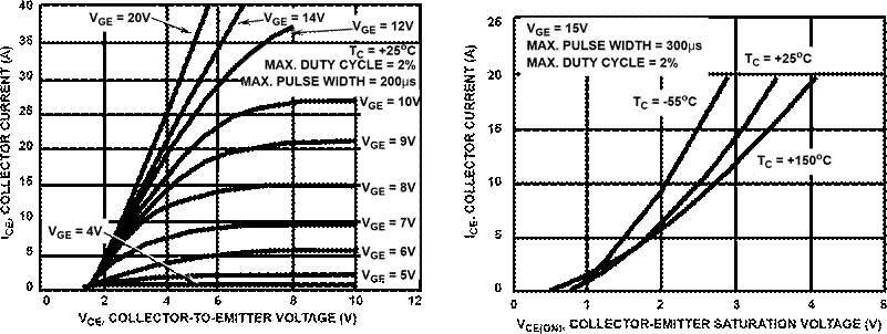
Absolute Maximum Ratings TC = +25oC, Unless Otherwise Specified
HGTB12N60D1C UNITS
Collector-Emitter Voltage (VGE = 0V). . . . . . . . . . . . . . . . . . . . . . . . . . . . . . . . . . . . . . . . .VCES 600 V
Collector-Gate Voltage (RGE = 1MΩ). . . . . . . . . . . . . . . . . . . . . . . . . . . . . . . . . . . . . . . . VCGR 600 V
 Collector
Current Continuous at TC = +100oC . . .
. . . . . . . . . . . . . . . . . . . . . . . . . . . . . . . . . IC 12 A
at TC = +25oC . . .
. . . . . . . . . . . . . . . . . . . . . . . . . . . . . . . . . . IC 18 A
Collector Current Pulsed (Note 1) . . . . . . . . . . . . . . . . . . . . . . .
. . . . . . . . . . . . . . . . . . . . . ICM 40 A
Gate-Emitter Voltage . . . . . . . . . . . . . . . . . . . . . . . . . . . . .
. . . . . . . . . . . . . . . . . . . . . . . . VGE ±25 V
Collector
Current Continuous at TC = +100oC . . .
. . . . . . . . . . . . . . . . . . . . . . . . . . . . . . . . . IC 12 A
at TC = +25oC . . .
. . . . . . . . . . . . . . . . . . . . . . . . . . . . . . . . . . IC 18 A
Collector Current Pulsed (Note 1) . . . . . . . . . . . . . . . . . . . . . . .
. . . . . . . . . . . . . . . . . . . . . ICM 40 A
Gate-Emitter Voltage . . . . . . . . . . . . . . . . . . . . . . . . . . . . .
. . . . . . . . . . . . . . . . . . . . . . . . VGE ±25 V
Power Dissipation Total at TC = +25oC . . . . . . . . . . . . . . . . . . . . . . . . . . . . . . . . . . . . . . . . PD 75 W
Power Dissipation Derating TC > +25oC . . . . . . . . . . . . . . . . . . . . . . . . . . . . . . . . . . . . . . . . . . 0.6 W/oC Operating and Storage Junction Temperature Range . . . . . . . . . . . . . . . . . . . . . . . . .TJ, TSTG -55 to +150 oC
Thermal Resistance, Junction to Case. . . . . . . . . . . . . . . . . . . . . . . . . . . . . . . . . . . . . . . . RθJC 1.67 oC/W
Maximum Lead Temperature for Soldering . . . . . . . . . . . . . . . . . . . . . . . . . . . . . . . . . . . . . .TL 260 oC (1/8 inch from case for 5s)
NOTE: 1. Repetitive Rating: Pulse width limited by maximum junction temperature. Gate control turn-off not allowed above 50A.
HARRIS SEMICONDUCTOR IGBT PRODUCT IS COVERED BY ONE OR MORE OF THE FOLLOWING U.S. PATENTS:
4,364,073 4,417,385 4,430,792 4,443,931 4,466,176 4,516,143 4,532,534 4,567,641
4,587,713 4,598,461 4,605,948 4,618,872 4,620,211 4,631,564 4,639,754 4,639,762
4,641,162 4,644,637 4,682,195 4,684,413 4,694,313 4,717,679 4,743,952 4,783,690
4,794,432 4,801,986 4,803,533 4,809,045 4,809,047 4,810,665 4,823,176 4,837,606 4,860,080 4,883,767 4,888,627 4,890,143 4,901,127 4,904,609 4,933,740 4,963,951
4,969,027
CAUTION: These devices are sensitive to electrostatic discharge. Users should follow proper ESD Handling Procedures. File Number 2326.3
Copyright © Harris Corporation 1995
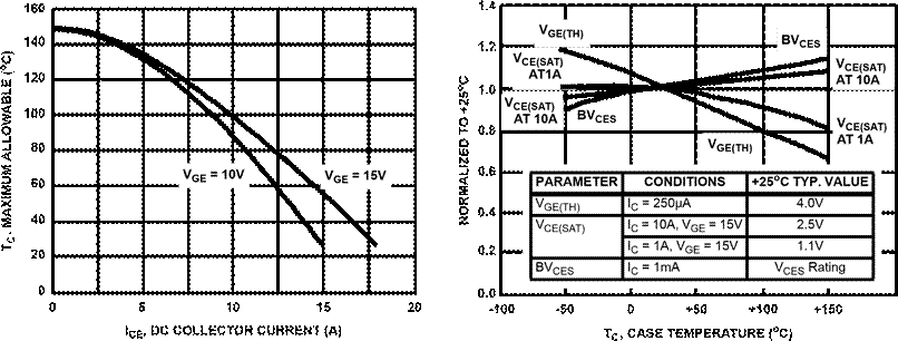
Electrical Specifications TC = +25oC, Unless Otherwise Specified
|
PARAMETERS |
SYMBOL |
TEST CONDITIONS |
LIMITS |
UNITS |
|||
|
MIN |
TYP |
MAX |
|||||
|
OFF CHARACTERISTICS |
|||||||
|
Collector-Emitter Breakdown Voltage |
BVCES |
IC = 25µA, VGE = 0V |
600 |
- |
- |
V |
|
|
Collector Cut-Off Current |
ICES |
TC = +25oC, VGE = 0V, VCE = Maximum Rating |
- |
- |
250 |
µA |
|
|
TC = +150oC, VGE = 0V, VCE = Maximum Rating x 0.8 (Note 1) |
- |
- |
4 |
mA |
|||
|
Gate-Emitter Leakage Current |
IGES |
VGE = ±20V |
- |
- |
±500 |
nA |
|
|
ON CHARACTERISTICS (Note 2) |
|||||||
|
Gate Threshold Voltage |
VGE(TH) |
VCE = VGE, IC = 250µA |
TC = +25oC |
2 |
4 |
5 |
V |
|
TC = +150oC |
- |
2.5 |
- |
V |
|||
|
Collector-Emitter Saturation Voltage |
VCE(SAT) |
VGE = 15V, IC = 10A, TC = +25oC |
- |
2.5 |
2.7 |
V |
|
|
VGE = 15V, IC = 10A, TC = +150oC |
- |
2.8 |
- |
V |
|||
|
VGE = 10V, IC = 10A, TC = +25oC |
- |
2.9 |
- |
V |
|||
|
DYNAMIC CHARACTERISTICS |
|||||||
|
Input Capacitance |
CIES |
VGE = 0V, VCE = 25V, f = 1MHz |
- |
1050 |
- |
pF |
|
|
Output Capacitance |
COES |
- |
340 |
- |
pF |
||
|
Reverse Transfer Capacitance |
CRES |
- |
10 |
- |
pF |
||
|
SWITCHING CHARACTERISTICS (See Figures 8 and 9) (Note 2) |
|||||||
|
Turn-On Delay Time |
tD(ON) |
Resistive Load, TJ = +125oC, IC = 10A, VCE = 500V, VGE = 15V, RG(ON) = 50Ω, RG(OFF) = 100Ω |
- |
100 |
- |
ns |
|
|
Rise Time |
tR |
- |
100 |
- |
ns |
||
|
Turn-Off Delay Time |
tD(OFF) |
- |
0.4 |
- |
µs |
||
|
Fall Time |
tF |
- |
2.5 |
- |
µs |
||
|
Turn-Off Delay Time |
tD(OFF)I |
Inductive Load, TJ = +125oC, L = 45µH, IC = 10A, VCE(CLAMP) = 500V, VGE = 15V, RG(ON) = 50Ω, RG(OFF) = 100Ω |
- |
0.8 |
1.2 |
µs |
|
|
Fall Time |
tFI |
- |
0.8 |
1.0 |
µs |
||
|
Equivalent Fall Time |
tF(EQ) |
- |
0.6 |
0.8 |
µs |
||
|
Turn-Off Switching Losses |
WOFF |
- |
1.6 |
2.0 |
mJ |
||
|
PILOT CHARACTERISTICS (Notes 2, 3 and 4) |
|||||||
|
Pilot-Emitter Kelvin Voltage |
VPEK |
VGE = 15VDC, RP = 2kΩ |
|||||
|
IC = 5A |
- |
1.25 |
- |
V |
|||
|
IC = 10A |
1.4 |
1.67 |
1.8 |
V |
|||
|
IC = 20A |
- |
2.06 |
- |
V |
|||
NOTES:
1. Applies for 3.3 oC per watt maximum thermal resistance, case-to-ambient.
2. Pulse test: Pulse widths ≤ 300µs, duty cycle ≤ 2%.
3. Refer to Figure 10.
4. When not in use connect S to emitter.
HGTB12N60D1C
5 10 20 30
ICE, EMITTER CURRENT (A)
0 100 200 300 400 500
VCE, COLLECTOR-EMITTER VOLTAGE (V)
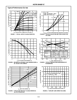
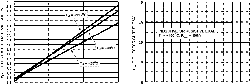
FIGURE 6. TURN-OFF SAFE OPERATING AREA
HGTB12N60D1C
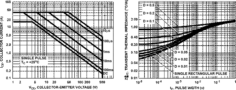
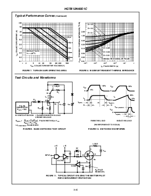
FIGURE 7. TURN-ON SAFE OPERATING AREA FIGURE 8. MAXIMUM TRANSIENT THERMAL IMPEDANCE
![]()
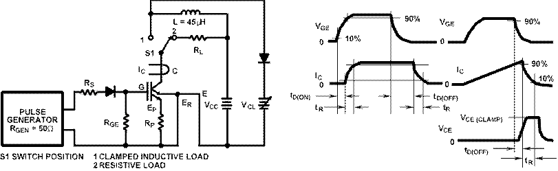
RG(ON) = (RGEN + RS)(RGE) PULSE WIDTH 60µs VCC RESISTIVE LOAD INDUCTIVE
Уважаемый посетитель!
Чтобы распечатать файл, скачайте его (в формате Word).
Ссылка на скачивание - внизу страницы.