|
Peak diode voltage |
1 MV |
|
Ion-beam energy density |
50 ~ 100 J/cm2 |
|
Pulse width |
~ 50 ns |
|
Ion species |
H+ (80 %) |
|
Beam spot size |
~ f 15 mm |
|
Target-substrate distance |
40 ~ 100 mm |
|
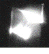
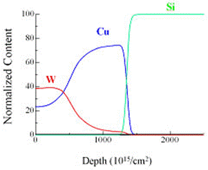
Hybrid target is used to observe the properties of the ablation plasma. Figure 4a shows the setup of the experiment. Two kinds of metal material, copper and tungsten, are used to form a hybrid target of periodic structure with a pitch of 1 mm. The intent of this experiment is to ablate two targets with the same ion beam so that the ablation plasmas can mix with each other. The high-speed photograph in Figure 4b shows the plasma movement between the target and the substrate, but without any information on the species of the material. However, the thin-film profile obtained by the Rutherford back-scattering (RBS), shown in Figure 4c, indicates that the thin film is not a uniform mixture of Cu and W. Instead, copper covers most of the bottom layer adjacent to the substrate. This result is explained by the fact that the copper target is ablated earlier than tungsten because of its lower melting and boiling temperatures.
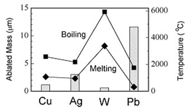
Figure 3. Ablated target mass and target boiling and melting temperatures The ablation plasma carries a large amount of thermal energy to the substrate. This effect is very important in forming crystalline structure in the thin film deposited on a substrate without external heating. The thermal influence on the thin-film deposition can be seen from the surface morphology of the metal thin films.
a) b) c) Figure 4. a) Experimental setup for Cu-W hybrid target; b) high-speed photograph; c) thin-film profile obtained by RBS
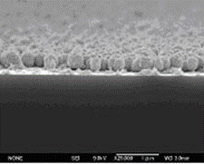
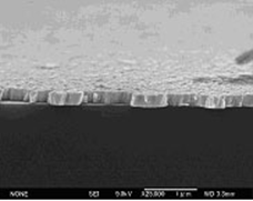
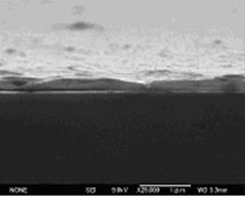
r=0 r=20 mm r=50 mm Figure 5. SEM photographs of the silver thin films obtained at different substrate positions Figure 5 shows the scanning electron microscope (SEM) photographs obtained at different positions on the substrate, where r is the distance from the center of the plasma plume. Since different position corresponds to different thermal impact by the ablation plasma, each silver thin film shown in Figure 5 exhibits unique structure and surface morphology. This dependence is clearly seen for metal thin films who have relatively low melting and boiling temperatures. References 1. Shimotori Y., Yokoyama M., Isobe H., Harada S., Masugata K., Yatsui K., Journal of Applied Physics, 63, 968–970, 1988. 2. Yatsui K., Kang X. D., Sonegawa T., Matsuoka T., Masugata K., Shimotori Y., Satoh T., Furuuchi S., Ohuchi Y., Takeshita T., Yamamoto H., Physics of Plasmas, 1, 1730–1737, 1994. 3. Renk T. J., Provencio P. P., Prasad S. V., Shlapakovski A. S., Petrov A. V., Yatsui K., Jiang W., Suematsu H., Proceedings of the IEEE, 92, 1057–1081, 2004. 4. Jiang W., Hashimoto N., Shinkai H., Ohtomo K., Yatsui K., Nuclear Instruments, Methods in Physics Research, A 415, 533–538, 1998. 5. Jiang W., Hashimoto N., Yatsui K., IEEE Transactions on Plasma Science, 28, 1549–1552, 2000. 6. Jiang W., Ide K., Kitayama S., Suzuki T., Yatsui K., Japanese Journal of Applied Physics, 40, 1026–1029, 2001. |
Уважаемый посетитель!
Чтобы распечатать файл, скачайте его (в формате Word).
Ссылка на скачивание - внизу страницы.
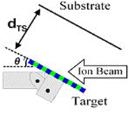
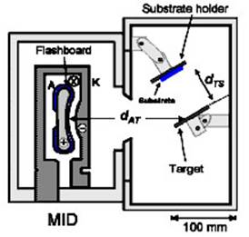 Figure 2.
Experimental setup of
thin-film deposition by IBE
Figure 2.
Experimental setup of
thin-film deposition by IBE