

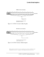

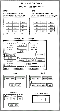
B CONTROL/STATUS REGISTERS
Figure B-0.
Table B-0.
Listing B-0.
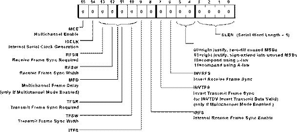
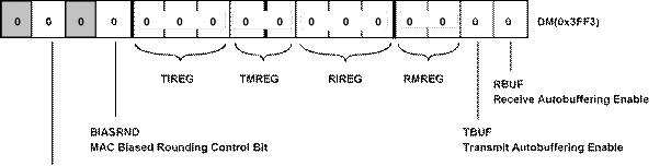
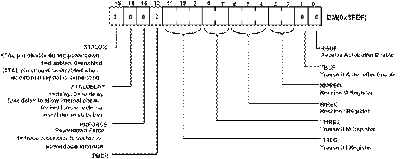
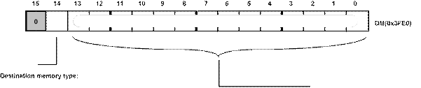
This appendix shows bit definitions for ADSP-218x memory-mapped control registers and non-memory-mapped control and status registers.
The memory-mapped registers are listed in
descending address order. Default bit values at reset are shown. If no value is
shown, the bit is undefined at reset. Reserved bits are shown on a grey field.
These reserved bits must be set to zero.
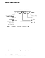
|
0X3FFD 0X3FFC 0X3FFB |
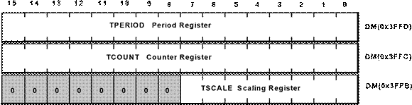
TPERIOD |
|
|
TCOUNT |
||
|
TSCALE |
|
0X3FFF 0X3FFE 4 |
SYSTEM CONTROL REGISTER |
||
|
WAIT STATES |
|||
|
4 |
|||
|
DMOVLAY |
PMOVLAY |
||
|
MULTICHANNEL ENABLES
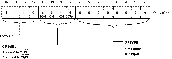
0X3FFA 0X3FF9 0X3FF8 0X3FF7 SPORT0 CONTROL |
|||||
|
0X3FF6 0X3FF5 0X3FF4 0X3FF3 |
CONTROL |
||||
|
SCLKDIV |
|||||
|
RFSDIV |
|||||
|
AUTOBUFFER |
|||||
|
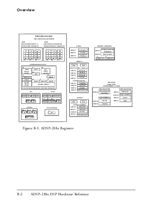
IDMA REGISTERS
0X3FE0 PROGRAMMABLE FLAG REGISTERS
0X3FE6 0X3FE5 |
BDMA REGISTERS
0X3FE4 0X3FE3 0X3FE2 0X3FE1 |
|
SPORT1 CONTROL 0X3FF2 CONTROL |
|
|
0X3FF1 0X3FF0 0X3FEF |
SCKLDIV |
|
RFSDIV |
|
|
AUTOBUFFER |
|
 TIMER MEMORY
INTERFACE
TIMER MEMORY
INTERFACE
SPORT 0
IDMA PORT
BDMA PORT
PROGRAMMABLE FLAGS
SPORT 1
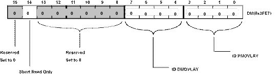
Figure B-1. ADSP-218x Registers
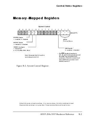
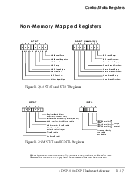
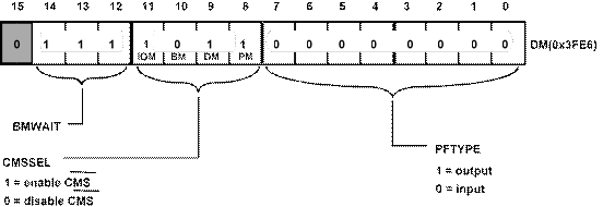
System Control
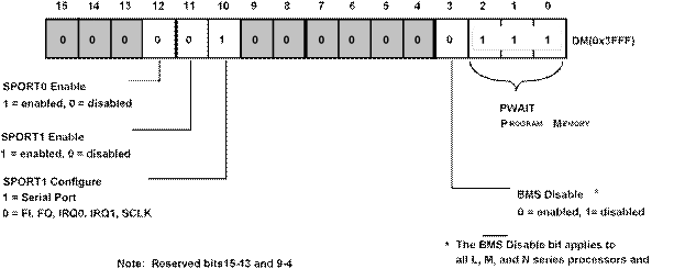
must always be set to 0. the ADSP-2184 and ADSP-2186
processors. This bit is unused in all other ADSP-218x processors and should be set to 0.
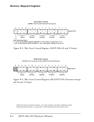
(ADSP-218x M and N Series Processors)
Wait State Mode Select
0 = normal mode (PWAIT, DWAIT, IOWAIT0-3 = N wait states, ranging from 0 to 7)
1= 2N+1 mode (PWAIT, DWAIT, IOWAIT0-3 = 2N+1 wait states, ranging from 0 to 15)
(All ADSP-218x Processors except ADSP-218x M and N Series)
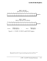
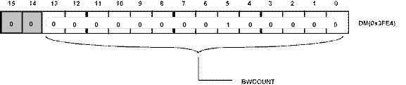
15 14 13 12 11 10 9 8 7 6 5 4 3 2 1 0
 DM(0x3FFE)
DWAIT IOWAIT3 IOWAIT2 IOWAIT1 IOWAIT0
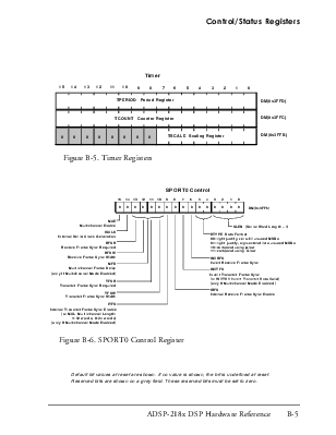
Timer
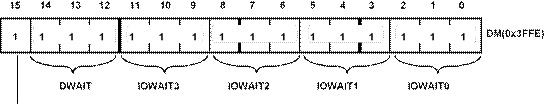
SPORT0 Control
 DM(0x3FF6)
DTYPE Data Format
Internal Transmit Frame Sync Enable (or MCL Multichannel Length:
1=32 words, 0=24 words)
(only If Multichannel Mode Enabled)
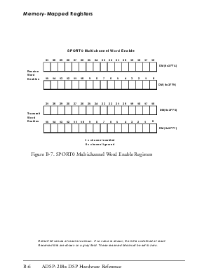
SPORT0 Multichannel W ord Enable
|
31 |
30 |
29 |
28 |
27 |
26 |
25 |
24 |
23 |
22 |
21 |
20 |
19 |
18 |
17 |
16 |
|
15 |
14 |
13 |
12 |
11 |
10 |
9 |
8 |
7 |
6 |
5 |
4 |
3 |
2 |
1 |
0 |
|
31 |
30 |
29 |
28 |
27 |
26 |
25 |
24 |
23 |
22 |
21 |
20 |
19 |
18 |
17 |
16 |
|
15 |
14 |
13 |
12 |
11 |
10 |
9 |
8 |
7 |
6 |
5 |
4 |
3 |
2 |
1 |
0 |
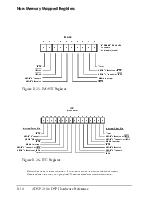
DM(0x3FFA)
Receive
W ord
Enables
DM(0x3FF9)
DM(0x3FF8)
Transmit W ord
Enables
DM(0x3FF7)
1 = channel enabled
0 = channel ignored
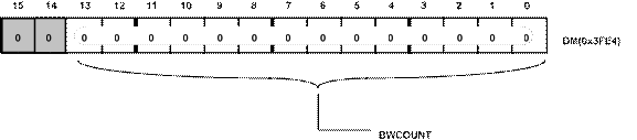
15 14 13 12 11 10 9 8 7 6 5 4 3 2 1 0
CLKODIS
CLKOUT Disable Control Bit
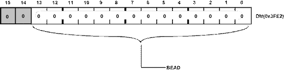
15 14 1 3 1 2 11 10 9 8 7 6 5 4 3 2 1 0
![]() DM(0x3FF5)
DM(0x3FF5)
|
15 |
1 4 |
1 3 |
SPORT0 RFSDIV Receive Frame Sync Divide Modulus 12 1 1 1 0 9 8 7 6 5 4 |
3 |
2 |
1 |
0 |
![]() DM(0x3FF4)
DM(0x3FF4)
|
SCLKDIV = |
CLKOUT frequency
2 * (SCLK frequency) |
– 1 |
RFSDIV = |
SCLKfrequency
RFS frequency |
– 1 |
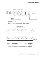
SPORT1 Control
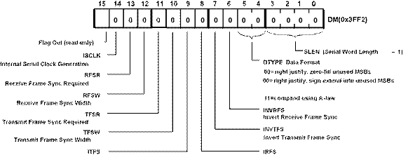 10=compand using µ
-law
10=compand using µ
-law
Internal Transmit Frame Sync Enable Internal Receive Frame Sync Enable
SPORT1 SCLKDIV
Serial Clock Divide Modulus
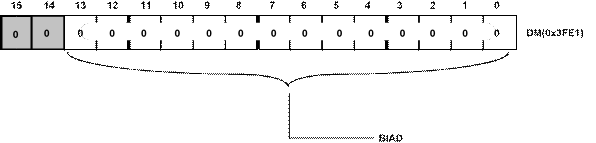
1 5 1 4 1 3 1 2 1 1 10 9 8 7 6 5 4 3 2 1 0
![]() DM(0x3FF1)
DM(0x3FF1)
|
1 5 |
1 4 |
1 3 |
1 2 |
SPORT1 RFSDIV Receive Frame Sync Divide Modulus 1 1 1 0 9 8 7 6 5 4 3 |
2 |
1 |
0 |
![]() DM(0x3FF0)
DM(0x3FF0)
|
SCLKDIV = |
CLKOUT frequency
2 * (SCLK frequency) |
– 1 |
RFSDIV = |
SCLK frequency
RFS frequency |
– 1 |
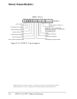
SPORT1 Autobuffer Control
Powerup Context Reset
1=soft reset (clear context)
0=resume execution
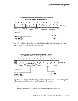
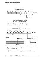
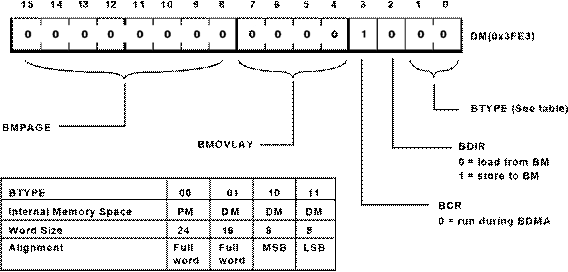
Programmable Flag and Composite Select Control
Programmable Flag and Composite Select Control
15 14 13 12 11 10 9 8 7 6 5 4 3 2 1 0
|
0 |
0 |
0 |
0 |
0 |
0 |
0 |
0 |
|||||||||
DM(0x3FE5)

Note: At reset the programmable flag pins PF7-PF0 are inputs. Therefore, the value of the PFDATA bit field is determined by the pin inputs (externally driven) at reset.
(ADSP-2187, ADSP-2188, and ADSP-2189)
 1 =
halt during BDMA,
1 =
halt during BDMA,
Context Reset when done
(All ADSP-218x Processors except ADSP-2187, ADSP-2188, and ADSP-2189)
 1 =
halt during BDMA,
1 =
halt during BDMA,
Context Reset when done
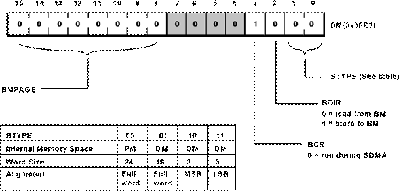
B D M A W ord C ount
M M A P =0 and B M O D E =0 (A D S P -2181 and A D S P -2183 only)
M O D E B =0 (A ll oth er A D S P -2 18x proc essors)
M M A P =1 or B M O D E =1 (A D S P -2181 and A D S P -2183 only)
M O D E B =1 (A ll oth er A D S P -2 18x proc essors)
N ote: B its 14 and 15 a re unusedand should be set to 0.
Note: B its 14 and 15 are unused and should be set to 0.
N ote: B its 14 and 15 are unused and should be set to 0.
IDMA Control
 IDMAD
IDMAD
0=PM IDMAA
1=DM Starting address
Note: Bit 15 is a reserved bit and should be set to 0 in all ADSP-218x processors except the ADSP-2187, ADSP-2188, and ADSP-2189.
ID M A O verlay
0 = D isa ble, 1 = E nable
N ote 1: The ID D M O V LA Y and ID P M O V LA Y bit fields apply onl y to the A D S P -2187, A D S P 2188, and A D S P -218 9 process ors. For all othe r A D S P -21 8x proce ssors, th ese bits are unused and m us t be set to 0.
N ote 2: The short read on ly bit (bit 14) applies to M and N se ries only.
For all othe r A D S P -218x processors , this bit is unused
Уважаемый посетитель!
Чтобы распечатать файл, скачайте его (в формате Word).
Ссылка на скачивание - внизу страницы.