


9 AC’97 CODEC PORT
Figure 9-0.
Table 9-0.
Listing 9-0.
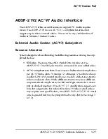
AC’97 is a digital interface for the transport of audio and modem samples that was originally developed by Analog Devices, Creative Labs, Intel, National Semiconductor, and Yamaha and documented in the AC’97 specification. For ADSP-2192, the AC’97 specification provides a high audio architecture for the 1997 and 1998 volume platform segments.
The AC’97 interface, which complies with the AC’97 specification, connects the host's Digital Controller (DC) chip set and one to four analog audio (AC), modem (MC), or Audio/Modem (AMC) codecs.
The AC’97 interface has the following features and functionality:
• Each DSP core within the ADSP-2192 has four FIFOs, which provide data communication paths to the remainder of the chip
• TX0, RX0, TX1, and RX1 are the FIFO registers in the universal register map of the DSP
A DSP-2192 Fe a ture s a nd Func tiona lity
• Each FIFO is eight words deep and 16 bits wide:
• Two FIFOs (RX0 and RX1) are inputs that receive data and send it to the DSP core
• Two FIFOs (TX0 and TX1) are outputs that send data from the DSP to the AC’97 interface
|
! |
The AC’97 interface read data is transmitted in a format of 20 bits per slot; however, the ADSP-2192 stores data in a 16-bit format. On slots 2 through 11, the AC’97 reads the 16 MSBs of the data and ignores the 4 LSBs.
• Interrupts can be generated when some number of words have been received in the receive FIFOs or when some number of words are empty in the transmit FIFOs
• FIFOs 0(TX0 and RX0) and 1 (TX1 and RX1) in each DSP core can be used to send and receive data to the AC'97 interface of the
ADSP-2192
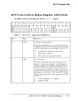
• Each FIFO has a 16-bit control register (STCTL0/1 and SRCTL0/1) associated with it:
• STCTL0/1 are the transmit FIFO control and status registers
• SRCTL0/1 are the receive FIFO control and status registers
Table 9-1. FIFO Receive and Control Status Registers
|
Address |
Register |
|
0x10 |
STCTL0 |
|
0x20 |
STCTL1 |
|
0x11 |
SRCTL0 |
Table 9-1. FIFO Receive and Control Status Registers
|
Address |
Register |
|
0x21 |
SRCTL1 |
|
0x12 |
TX0 |
|
0x22 |
TX1 |
|
0x13 |
RX0 |
|
0x23 |
RX1 |
! All bits in this register are reset to zero.
The following are the bit descriptions for the STCTL0/1 register:
|
15 |
14 |
13 |
12 |
11 |
10 |
9 |
8 |
7 |
6 |
5 |
4 |
3 |
2 |
1 |
0 |
|
|
|
|
|
|
|
|
|
|
|
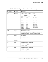
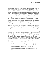
Table 9-2. STCTL0/1Register Bit Description
|
Bit Position |
Bit Name |
Description |
||
|
01:0 |
CE[1:0] |
Connection Enable 00 = Disable 01 = Reserved 10 = Connect to AC’97 11 = Reserved |
||
|
2 |
Reserved |
|||
|
3 |
SMSEL |
Stereo / Monaural Select - AC’97 Mode. 0 = Monaural Stream 1 = Stereo Stream |
||
|
7:4 |
SLOT[3:0] |
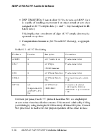
AC’97 Slot Select - AC’97 Mode Monaural Stereo 0000 -> 0010 = Reserved 0011 = Slot 3 Slots 3/4 |
||
|
0100 = |
Slot 4 |
Slots 4/5 |
||
|
0101 = |
Slot 5 |
Slots 5/6 |
||
|
0110 = |
Slot 6 |
Slots 6/7 |
||
|
0111 = |
Slot 7 |
Slots 7/8 |
||
|
1000 = |
Slot 8 |
Slots 8/9 |
||
|
1001 = |
Slot 9 |
Slots 9/10 |
||
|
1010 = |
Slot 10 |
Slots 10/11 |
||
|
1011 = |
Slot 11 |
Slots 11/12 |
||
|
1100 = |
Slot 12 |
Not Allowed |
||
|
1101 -> 1111 = Reserved |
||||
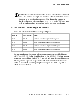
|
10:8 |
FIP[2:0] |
FIFO Interrupt Position. An interrupt is generated when FIP[2:0] +1 words are empty in the FIFO. The Interrupt is Level Sensitive. |
||
|
11 |
DME |
DMA Enable. 0 = DMA Disabled 1 = DMA Enabled |
||
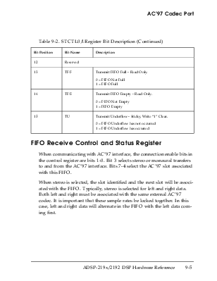
Table 9-2. STCTL0/1Register Bit Description (Continued)
|
Bit Position |
Bit Name |
Description |
|
12 |
Reserved |
|
|
13 |
TFF |
Transmit FIFO Full - Read Only. 0 = FIFO Not Full 1 = FIFO Full |
|
14 |
TFE |
Transmit FIFO Empty - Read Only. 0 = FIFO Not Empty 1 = FIFO Empty |
|
15 |
TU |
Transmit Underflow - Sticky, Write “1” Clear. 0 = FIFO Underflow has not occurred 1 = FIFO Underflow has occurred |
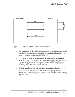
When communicating with AC’97 interface, the connection enable bits in the control register are bits 1-0. Bit 3 selects stereo or monaural transfers to and from the AC’97 interface. Bits 7-4 select the AC’97 slot associated with this FIFO.
When stereo is selected, the slot identified and the next slot will be associated with the FIFO. Typically, stereo is selected for left and right data. Both left and right must be associated with the same external AC’97 codec. It is important that these sample rates be locked together. In this case, left and right data will alternate in the FIFO with the left data coming first.
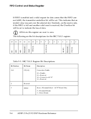
If FIFO is enabled and a valid request for data comes that the FIFO cannot fulfill, the transmitter underflow bit will be set. This indicates that an invalid value was sent over the selected slot. Similarly, on the receive side, if the FIFO is full and another valid word is received, the Overflow bit will be set to indicate the loss of data.
! All bits in this register are reset to zero.
The following are the bit descriptions for the SRCTL0/1 register:
|
15 |
14 |
13 |
12 |
11 |
10 |
9 |
8 |
7 |
6 |
5 |
4 |
3 |
2 |
1 |
0 |
|
|
|
|
|
|
|
|
|
|
|
Table 9-3. SRCTL0/1 Register Bit Descriptions
|
Bit Position |
Bit Name |
Description |
|
01:0 |
CE[1:0] |
Connection Enable. 00 = Disable 01 = Reserved 10 = Connect to AC’97 11 = Reserved |
|
2 |
Reserved |
|
|
3 |
SMSel |
Stereo / Monaural Select - AC’97 Mode Only. 0 = Monaural Stream 1 = Stereo Stream |
Table 9-3. SRCTL0/1 Register Bit Descriptions (Continued)
|
Bit Position |
Bit Name |
Description |
||
|
7:4 |
SLOT[3:0] |
AC’97 Slot Select - AC’97 Mode Monaural |
Only. Stereo |
|
|
0000 -> 0010 = Reserved 0011 = Slot 3 |
Slots 3/4 |
|||
|
0100 = |
Slot 4 |
Slots 4/5 |
||
|
0101 = |
Slot 5 |
Slots 5/6 |
||
|
0110 = |
Slot 6 |
Slots 6/7 |
||
|
0111 = |
Slot 7 |
Slots 7/8 |
||
|
1000 = |
Slot 8 |
Slots 8/9 |
||
|
1001 = |
Slot 9 |
Slots 9/10 |
||
|
1010 = |
Slot 10 |
Slots 10/11 |
||
|
1011 = |
Slot 11 |
Slots 11/12 |
||
|
1100 = |
Slot 12 |
Not Allowed |
||
|
1101 -> 1111 = Reserved |
||||
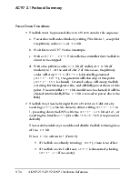
|
10:8 |
FIP[2:0] |
FIFO Interrupt Position. An interrupt is generated when FIP[2:0] + 1 words have been Received in the FIFO. The interrupt is level sensitive. |
||
|
11 |
DME |
DMA Enable. 0 = DMA Disabled 1 = DMA Enabled |
||
|
12 |
Reserved |
|||
|
13 |
RFF |
Receive FIFO Empty - Read Only. 0 = FIFO Not Empty 1 = FIFO Empty |
||
|
14 |
RFE |
Receive FIFO Empty - Read Only. 0 = FIFO Not Empty 1 = FIFO Empty |
||
Table 9-3. SRCTL0/1 Register Bit Descriptions (Continued)
|
Bit Position |
Bit Name |
Description |
|
15 |
RO |
Receive Overflow - Sticky, Write-One-Clear. 0 = FIFO Overflow has not occurred 1 = FIFO Overflow has occurred |
|
0x48 |
TX0ADDR |
|
0x4C |
RX0ADDR |
|
0x50 |
TX1ADDR |
|
0x54 |
RX1ADDR |
This is the 16-bit register specifying the current address
Уважаемый посетитель!
Чтобы распечатать файл, скачайте его (в формате Word).
Ссылка на скачивание - внизу страницы.