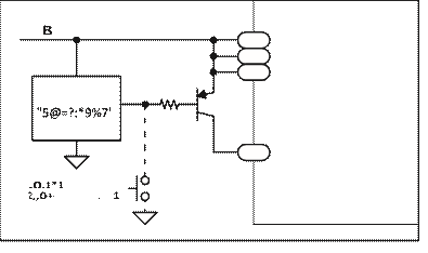
blocks at the left of these diagrams represent SFR bits in the SPI and I2C control registers (SPICON & I2CCON). Notice that in I2C mode (SPE=0) the upper FET in each diagram is held in its “off” state, thereby giving both pins “open drain” type drivers with no internal pull-up, as per standard I2C. By contrast, in SPI mode (SPE=1) the upper FET is controlled directly by SPI hardware, giving the pin push/pull capability. Also, in I2C mode (SPE=0) two pull-down FETs operate in parallel in order to provide an extra 60% or 70% of current sinking capability. In SPI mode, however, (SPE=1) the bottom FET in each diagram is disabled and only one pull-down FET operates on each pin, resulting in sink capabilities identical to that of port 0 and port 2 pins.
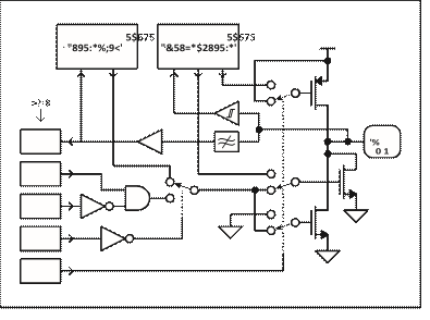
On the input path of SCLOCK and SDATA/MOSI, notice that a Schmitt trigger conditions the signal going to the SPI hardware to prevent false triggers (double triggers) on slow incoming edges. For incoming signals from these pins going to I2C hardware, a filter conditions the signals in order to reject glitches of up to 50ns in duration.
The functions of the “Hardware I2C” and “Hardware SPI” blocks of the above diagrams will be described in Chapter 3 of this manual. However, note that direct access to the SCLOCK and SDATA/MOSI pins is afforded through the SFR interface in I2C master mode. Therefore, if you are not using the SPI or I2C functions, you can use these two pins for general purpose I/0. The SDATA/MOSI pin can be used for both input and output, while the SCLOCK pin can only be used as an output in this mode.
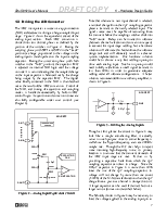
You must implement external POR (power-on reset) circuitry to drive the RESET pin of the ADuC812. Your circuit must hold the RESET pin asserted
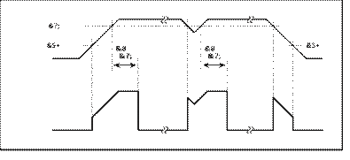
(high) whenever the power supply (AVDD & DVDD) is below 2.5V. Furthermore, VDD must remain above 2.5V for at least 10ms before the RESET signal is de-asserted (low). The external POR circuit must be operational down to 1.2 volts or less. The timing diagram of Figure 25 illustrates this functionality under three separate events: power-up, brownout, and power-down. Notice that when RESET is asserted (high) it tracks the voltage on VDD.
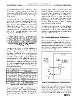
The best way to implement an external POR function to meet the above requirements involves the use of a dedicated POR chip, such as the ADM181x family of SOT-23 packaged PORs from Analog Devices. Recommended connection diagrams for both active-high and active-low type PORs are shown in Figure 26 and Figure 27 respectively. The POR chip’s output can also be used to provide reset signals to additional circuitry on your board that may need a POR, but be sure to observe the POR chip’s output loading limitations.
Some active-low POR chips, such as the ADM1813 & ADM1818, can be used with a manual pushbutton as an additional reset source as illustrated by the dashed line connection in Figure 27.
The recommended POR implementations of Figure 26 or Figure 27 will ensure correct startup and shutdown under virtually any power-cycling scenarios, including incomplete shutdown and brown-out conditions.
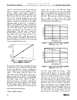
The ADuC812’s operational power supply voltage range is 2.7V to 5.5V. Though the guaranteed datasheet specifications are given only for power supplies within ±10% of nominal 3V or 5V levels, the chip will function equally well at any power supply level between 2.7V and 5.5V.
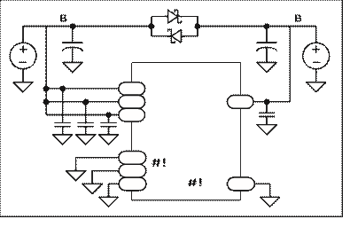
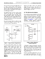
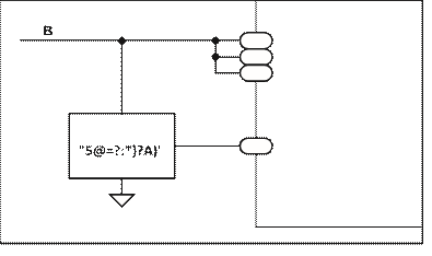
Figure 28 – Powering from Separate
Separate analog and digital power supply pins (AVDD and DVDD respectively) allow AVDD to be kept relatively free of noisy digital signals often present on the system DVDD line. However, though you can power AVDD and DVDD from two separate supplies if desired, you must ensure that they remain within ±0.3V of one another at all times in order to avoid damaging the chip (as per the absolute maximum ratings in the product datasheet).
Therefore, it is recommended that unless AVDD and DVDD are connected directly together, you connect back-to-back Schottky diodes between them, as shown in Figure 28.
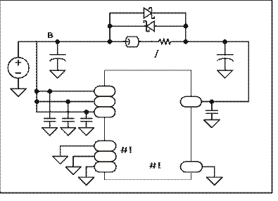
As an alternative to providing two separate power supplies, you can help keep AVDD quiet by placing a small series resistor and/or ferrite bead between it and DVDD, and then decoupling AVDD separately to ground. An example of this configuration is shown in Figure 29. Do not, however, use a series inductor between AVDD and DVDD to avoid
Уважаемый посетитель!
Чтобы распечатать файл, скачайте его (в формате Word).
Ссылка на скачивание - внизу страницы.