a
ADuC812 MicroConverter®
Parallel Programming Specification
Version 1.3
10 July 2001
This document details device configuration and timing specifications required to program the Flash/EE Memory of the ADuC812 MicroConverter in parallel programming mode. The ADuC812 datasheet includes other necessary product information not offered in this document. It can be found at http://www.analog.com/microconverter.
Note that parallel programming mode is only one of two methods to program the ADuC812. For details on the in-circuit serial download mode, refer to the ADuC812 datasheet and tech note uC004, both available at http://www.analog.com/microconverter.
Rise & Fall times on all timing diagrams in this document are specified as 10ns min / 100ns max. All timing parameters are measured from the 50% level on a given signal.
CONTENTS:
|
Section: |
Page: |
|
Pin Configuration |
2 |
|
Power-Up & Power-Down Sequences |
3 |
|
Memory Map |
4 |
|
Command Functions |
4 |
|
Read Device Signature |
5 |
|
Read Byte |
6 |
|
Erase All |
7 |
|
Program Byte |
8 |
|
Program Page |
9 |
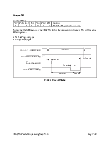
The basic pin configuration for parallel programming is shown in Figure 1. The specific function of each pin and port is outlined below.
• Port 0: 8-bit bi-directional DATA BUS for programming and reading bytes
• Ports 1 & 2: 16-bit ADDRESS BUS input (Port 1 is the high-byte, Port 2 is the low-byte)
• P3.1-P3.7: 7-bit COMMAND input, for specifying erase, program, read, etc.
• P3.0: active-low ENABLE COMMAND input for strobing a command on P3.1-P3.7
• ALE: active-low WRITE ENABLE input, used in programming functions
• EA : active-high ENABLE HV input, enables on-chip high-voltage charge-pump when high
•
![]() XTAL1: STROBE
CONFIG input, used to latch the chip into parallel programming mode
XTAL1: STROBE
CONFIG input, used to latch the chip into parallel programming mode
• PSEN : MODE SELECT input, used with XTAL1 to select parallel programming mode
• RESET: this pin must remain at the same potential as the VDD pins at all times
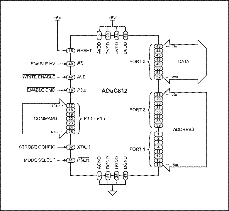
Figure 1: Pin Configuration for Parallel Programming
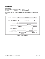
There are a number of requirements for correct application and removal of power for parallel programming mode. They are outlined in the below bullets and further details are illustrated in Figure 2.
• All four ground pins (DGND & AGND) must be treated as a single node.
• All four VDD pins (AVDD & DVDD) plus the RESET pin must all be treated as a single node.
• The voltage applied to any pin must never be greater than VDD or less than ground.
• Any time power is applied to the chip all signals must meet the requirements of Figure 2.
• During the “Command Sequences” section of Figure 2, the following reqirements must be met....
− VDD and RESET must remain high.
![]() − PSEN must remain low.
− PSEN must remain low.
− XTAL1 must remain low.
− ALE and P3.0 must remain high, except when pulsed low during specific command sequences.
![]() − EA must remain low,
except when pulsed high during specific command sequences.
− EA must remain low,
except when pulsed high during specific command sequences.
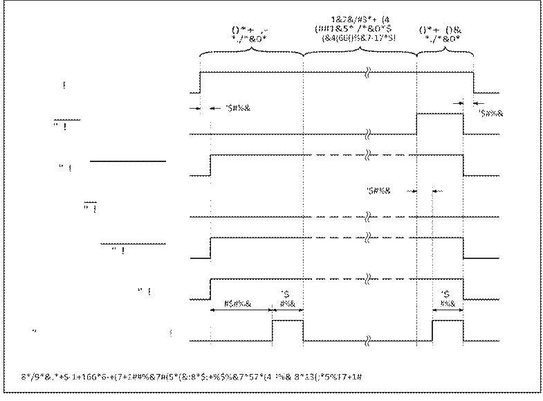
Figure 2: Power-Up & Power-Down Sequences for Parallel Programming
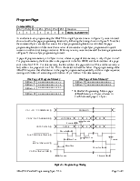
In parallel programming mode, the various areas of the ADuC812’s internal Flash/EE memory are mapped into portions of the 64K byte addressable space as shown in Figure 3.
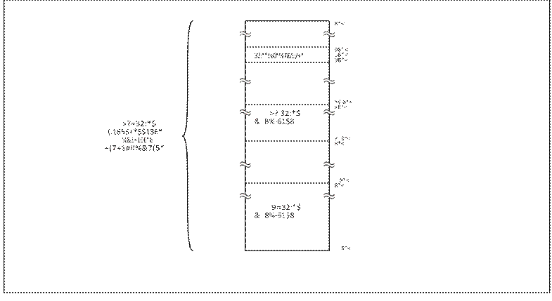
Figure 3: Parallel Programming Memory Map
The commands used to carry out various parallel programming functions are listed below.
|
P3.7 |
P3.6 |
P3.5 |
P3.4 |
P3.3 |
P3.2 |
P3.1 |
Function |
Page |
|
1 |
1 |
1 |
1 |
1 |
1 |
1 |
default pullups – do nothing |
– |
|
1 |
1 |
1 |
1 |
0 |
0 |
0 |
ERASE ALL (code/data plus security bits) |
7 |
|
1 |
1 |
1 |
1 |
0 |
0 |
1 |
READ DEVICE SIGNATURE |
5 |
|
1 |
1 |
1 |
1 |
0 |
1 |
0 |
PROGRAM BYTE |
8 |
|
1 |
1 |
1 |
1 |
0 |
1 |
1 |
READ BYTE |
6 |
|
all others |
reserved |
– |
||||||
Each of the above command functions is described in detail
Уважаемый посетитель!
Чтобы распечатать файл, скачайте его (в формате Word).
Ссылка на скачивание - внизу страницы.