|
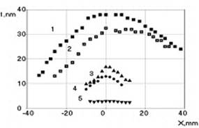
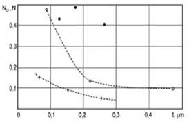
Application of High-Power Ion Beams to Thin Films Deposition and Stimulating Mass Transfer of Previously Implanted Dopants in Materials* Alexandr I. Ryabchikov, Vasily M. Matvienko, Anatoli V. Petrov, Vasily K. Struts, Yuri P. Usov, Anatoli S. Shlapakovski Nuclear Physics Institute at Tomsk Polytechnic University, 2a Lenin av., Tomsk 634050, Russia Abstract. The results of investigations concerning some applications of high-power ion beams (HPIBs) to materials surface modification are presented. For HPIB-based film deposition, the characteristics of obtained coatings were studied depending on deposition conditions. It has been shown that mechanical and adhesion properties of the films are improved with decreasing deposition rate. For the combined surface treatment comprising traditional ion implantation and HPIB irradiation, the mass transfer of implanted dopant was investigated at multiple implantation-irradiation cycles. It has been demonstrated that one can control the depth of occurrence and storage of the implanted dopant. INTRODUCTION Long-term studies of the features of HPIBs impact on materials have determined the main areas of their application to materials modification [1]. Among these areas are thin film deposition from ablation plasma and combined treatment, in particular, for the formation of deeply doped surface layers. Using HPIBs for an energetic impact in these applications has evident advantages in comparison with pulsed electron or laser beams due to the enhanced energy loss of ions in matter. In the first part of this work, we present the results of research on thin film formation at the ablation of different materials considering the variation of film properties with the key parameter of the process, the deposition rate. In the second part, investigations of HPIB-induced mass transfer of the implanted dopant at multiple cycles «conventional implantation — HPIB irradiation» are described. This kind of combined treatment is of interest also for the formation of the transition layers improving the adhesion of deposited coatings. THIN FILM DEPOSITION FROM ABLATION PLASMA It is well known that thin film deposition from the high-density, high-temperature, high-kinetic energy ablation plasma has such advantages as the highest productivity (up to 0.5 mm/shot; even for 1 pps rep-rate, it surpasses other methods, at least by 3 orders), substrate heating by plasma (no need in external heating), fast cooling of the surface layer (up to 109 K/s; important for nano-crystalline structure formation), and high-temperature chemical transformations (that can improve the adhesion). Less often mentioned disadvantages of the method are the occurrence of internal stresses in the film due to the difference between the linear expansion coefficients of the film and substrate materials and the high latent heat liberation during the crystallization leading to the formation of columnar structure in the film. The key parameter of the process determining these conditions of the film formation and, hence, influencing on the film properties is the deposition rate. We investigated the adhesion and mechanical properties of the films obtained using the HPIBs for ablation of carbon, copper, and titanium targets at the deposition rate varied within the range of 2 to 40 nm/shot. Experimental Conditions and Methods The silicon substrates made of Si (100) and having square (10´10 mm) or circular (Æ30 mm) form were installed onto the glass substrate, where the full deposition pattern was observed. The variation of the deposition rate was achieved by two means: changing the target-substrate distance dTS and using the different ablation areas. For ablation of the Ti target, we used the HPIB (70 % H+, 30 % C+, 350 keV, 60 ns, 5 J/cm2) of 25´40 mm size at the target (smaller dimension along the direction of ions motion) produced from the strip magnetically insulated diode with cylindrical (linear) focusing. To get larger cross-section of plasma flows, in case of ablation of Cu and C, we used the HPIB (70 % H+, 30 % C+, 500 keV, 100 ns, 8 J/cm2) produced from the Br-diode with conical focusing; at a target, it had the form of the oval (70´40 mm) elongated according to the beam propagation. The number of HPIB pulses set the desired film thickness. The film thickness was measured by Linnik interferometer, the adhesion, friction force, and friction coefficient were estimated using the CSEM scratch tester, the roughness was determined by the 3-D non-contact profilometer, and the nanohardness and Young modulus were measured by the CSEM nanohardness meter. Results In Figure 1, film thickness profiles (per one HPIB pulse) over the substrates are shown for Ti-Si and Cu-Si coatings obtained at different target-substrate distances. The character of dependences on dTS is different for the two systems. For Ti-Si films deposited using the «linear source», the profile flattens and the thickness decreases with increasing dTS due to the angular divergence of ablation plasma much faster compared to the case when the source with the large area of ablation was used. In Table 1, the characteristics of the thin films formed at different deposition rates with the use of the two sources are presented. One can see that film properties are continuously improved with increasing dTS. It is especially noticeable for the source giving the large ablation area at dTS=240 mm. An exception is the Cu-Si films, for which the nanohardness and Young modulus remain unchanged within the measurements accuracy. This is connected with the absence of different allotropic forms for Cu crystals, unlike C and Ti, for which these characteristics increase with increasing dTS due to the change of the film crystal structure. The same tendency of film properties variation was observed also in the transverse direction at each given distance dTS. Such film quality factors as the adhesion and friction behavior are also improved at a reduced deposition rate. For Ti-Si films of comparable thickness, the measured friction coefficient is 3 times lower in case of dTS=190 mm compared to that of dTS=55 mm. As to the adhesion, the critical indentation load in the scratch tester, at which the film begins to flake away off the substrate, is shown for Ti-Si films in Figure 2 as a function of the film thickness set by the number of HPIB pulses at different dTS. It is seen that the adhesion strength increases as the thickness decreases and with increasing dTS at the thickness given that is connected with the reduction of internal stresses in the films. For relatively thick coatings, adhesion can be improved by creating a transition layer in some optimal scheme of mixing film-substrate layers using the HPIB of reduced fluence. As is seen from Figure 2, the critical load for the Ti/Si film with the transition layer becomes up to 4 times as much. For the Cu-Si and C-Si films, the adhesion is also improved with increasing dTS. It should be noted that the critical loads, at which films begin to flake away are much greater for the C-Si and Ti-Si films than for the Cu-Si films. It is probably connected with the formation of chemical bonding between the film and substrate.
|
Уважаемый посетитель!
Чтобы распечатать файл, скачайте его (в формате Word).
Ссылка на скачивание - внизу страницы.