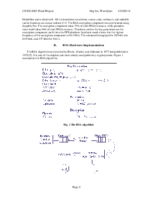
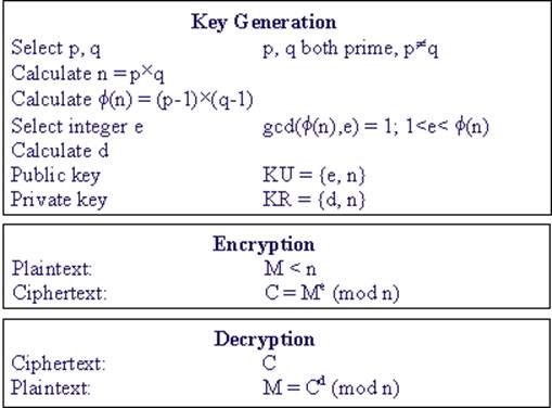
algorithm was inverted by Rivest, Shamir, and Adleman in 1977 and published in 1978 [5]. It is one of the simplest and most widely used public-key cryptosystems. Figure 1 summarizes the RSA algorithm.
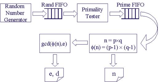
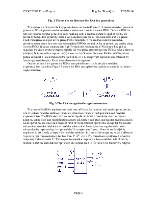
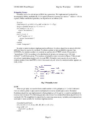
The system architecture for key generation is shown in Figure 2. A random number generator generates 512-bit pseudo random numbers and stores them in the rand FIFO. Once the FIFO is full, the random number generator stops working until a random number is pulled out by the primality tester. The primality tester takes a random number as input and tests if it is a prime. Confirmed primes are put in the prime FIFO. Similarly to the random number generator, primality tester starts new test only when prime FIFO is not full. A lot of power is saved by using the two FIFOs because computation is performed only when needed. When new key pair is required, the down stream component pulls out two primes from the prime FIFO, and calculates n and j(n). N is stored in a register. j(n) is sent to the Greatest Common Divider (GCD), where public exponent e is selected such that gcd(j(n), e) = 1, and private exponent d is obtained by inverting e modulo j(n). E and d are also stored in registers.
Once n, d, and e are generated, RSA encryption/decryption is simply a modular exponentiation operation. Figure 3 shows the RSA encryption/decryption structure in hardware implementation.
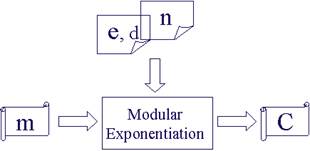
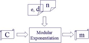
Fig. 3 The RSA encryption/decryption structure
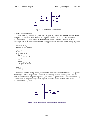
The core of the RSA implementation is how efficient the modular arithmetic operations are, which include modular addition, modular subtraction, modular multiplication and modular exponentiation. The RSA also involves some regular arithmetic operations, such as regular addition, subtraction and multiplication used to calculate n and j(n), and regular division used in GCD operation. We have implemented most of the mentioned operations, except for the regular subtraction, modular addition and modular subtraction. Instead, we use regular adder to do subtraction by representing the operands in 2's complement format. Omura's method [6] is employed to efficiently compute the modular addition. In his method temporary value is allowed to grow larger than modulus n but less than 2k (2k-1 < n < 2k), correction is performed when the temporary value exceeds 2k. Techniques for modular exponentiation, modular multiplication, modular addition, and addition operations are summarized in [7], which we found very helpful.
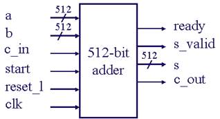
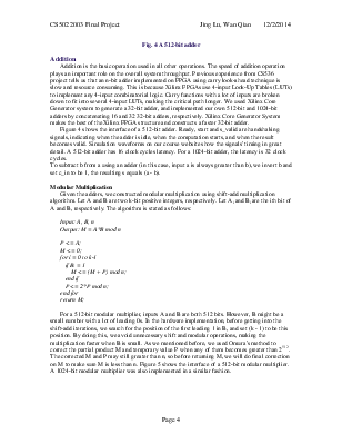
Addition is the basic operation used in all other operations. The speed of addition operation plays an important role on the overall system throughput. Previous experience from CS536 project tells us that an n-bit adder implemented on FPGA using carry look-ahead technique is slow and resource consuming. This is because Xilinx FPGAs use 4-input Look-Up Tables (LUTs) to implement any 4-input combinatorial logic. Carry functions with a lot of inputs are broken down to fit into several 4-input LUTs, making the critical path longer. We used Xilinx Core Generator system to generate a 32-bit adder, and implemented our own 512-bit and 1024-bit adders by concatenating 16 and 32 32-bit adders, respectively. Xilinx Core Generator System makes the best of the Xilinx FPGA structure and constructs a faster 32-bit adder.
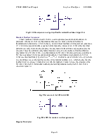
Figure 4 shows the interface of a 512-bit adder. Ready, start and s_valid are handshaking signals, indicating when the adder is idle, when the computation starts
Уважаемый посетитель!
Чтобы распечатать файл, скачайте его (в формате Word).
Ссылка на скачивание - внизу страницы.