5.45 Tracing Timing Violations
During the timing simulation (in VHDL), you may observe the glitch warning messages displayed in the Console window. An example of a warning is presented below:
WARNING: VitalGlitch: GLITCH Detected on port O;
Preempted Future Value := 1 @ 392.234 ns;
Newly Scheduled Value := 0 @ 392.709 ns;
Time: 390709 ps, Iteration: 2,
Instance: /UUT/U1_U1_P240_0_CO1_FGBLOCK_LUTRAM_FLUT_OR3.
Note: Glitch is a short pulse on a signal waveform that is usually undesired and may cause an unexpected design behavior.
5.46 Tracing Timing Violations
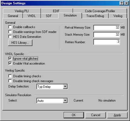
Active-HDL allows
you to disable
glitch detection by checking the
Ignore VITAL glitches option on
the Simulation tab of the Design
Settings window.
In the example, the glitch has been
detected on the O output port of the
/UUT/U1_U1_P240_0_CO1_FGBLOCK_LUTRAM_FLUT_OR3
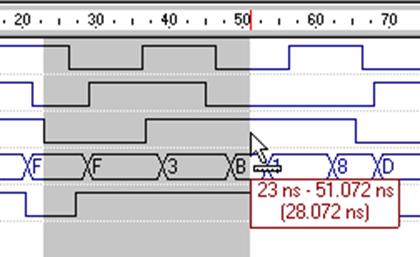
instance. To find out why it is not displayed in the Waveform Viewer
window, check if it is not caused by the unit transport delays.
Note: To disable the generation of messages during the training, use set -GMsgOn=false in the timing.do macro file.
5.47 Tracing Timing Violations
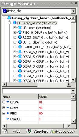
• To quickly locate the listed instance, switch to the Structure tab in the Design Browser window. Then, select Find from the pop-up menu.
• Right-click the top-level unit and enter U1_U1_P240_0_CO1_FGBLOCK_LUTRAM_FLUT_OR3 to locate the gate.
U1_U1_P240_0_CO1_FGBLOCK_LUTRAM_FLUT_OR3
By clicking on it, the Design Browser displays additional information in the lower part of the window.
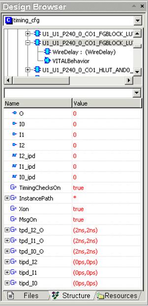
5.48 Tracing Timing Violations
As you can see, there are time structures of the VitalDelayType01 type. Each of these structures contains two time values:
– first, containing the time for signal transition from 0 to 1
– second, containing the time for signal transition from 1 to 0
The tipd_I1_O and tipd_I0_O structures hold time values for the input delays. This is the time after which a signal change is propagated from the input to the circuit.
The tpd_I1_O and tpd_I0_O structures hold time values for the output delays. This is the time after which signal change is propagated through the circuit to the output.
5.49 Tracing Timing Violations
Keeping in mind all of the above information, we can now explain what causes the glitch. In the warning displayed in the Console window, the time of the glitch detection is 390709 ps (390.709 ns). This is specified in the line beginning with the Time: clause:
WARNING:
VitalGlitch: GLITCH Detected on port O;
Preempted Future Value := 1 @ 392.234 ns;
Newly Scheduled Value := 0 @ 392.709 ns;
Time: 390709 ps, Iteration: 2,
Instance: /UUT/U1_U1_P240_0_CO1_FGBLOCK_LUTRAM_FLUT_OR3.
5.50 Tracing Timing Violations
The next preempted value for the output O port is '1' at 392.234 ns. However, the newly scheduled value for the output O port is '0' at 392.709 ns.
We should keep in mind that the current output value for the O port is '0'. The absolute time period between those two transactions equals 475ps and we know that the output delay for this particular gate is 2000ps.
If we add the present time value of 390709ps and the output delay of 2000ps then we will have the result of 392709ps. This is the time of the newly scheduled value for the output O port.
5.51 Tracing Timing Violations
However, the design operates in the VitalInertial transport mode where all input changes that have a duration time shorter than the output delay tpd are not propagated to the output and no glitch will appear at the output.
The simulator, therefore, does not display the glitch on the waveform. But it generates the warning that the glitch has been detected. Consequently, all glitch warnings can be explained this way.
5.52 Signal Alias Editor
The Signal Alias Editor is designed for creating and modifying signal aliases.
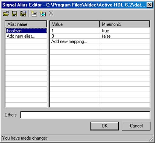
It can be used to:
• Create a new alias
• Create new value mappings for existing aliases
Уважаемый посетитель!
Чтобы распечатать файл, скачайте его (в формате Word).
Ссылка на скачивание - внизу страницы.