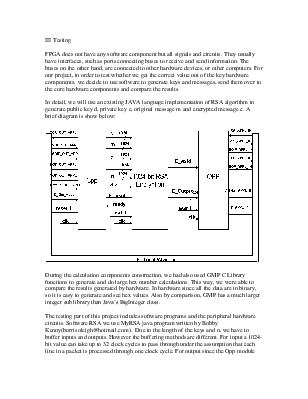
III Testing
FPGA does not have any software component but all signals and circuits. They usually have interfaces, such as ports connecting buses to receive and send information. The buses on the other hand, are connected to other hardware devices, or other computers. For our project, in order to test whether we get the correct value out of the key hardware components, we decide to use software to generate keys and messages, send them over to the core hardware components and compare the results.
In detail, we will use an existing JAVA language implementation of RSA algorithm to generate public key d, private key e, original message m and encrypted message c. A brief diagram is show below:
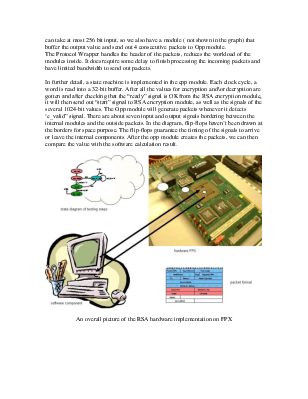
During the calculation components construction, we had also used GMP C Library functions to generate and do large hex number calculations. This way, we were able to compare the results generated by hardware. In hardware since all the data are in binary, so it is easy to generate and see hex values. Also by comparison, GMP has a much larger integer sub library than Java’s BigInteger class.
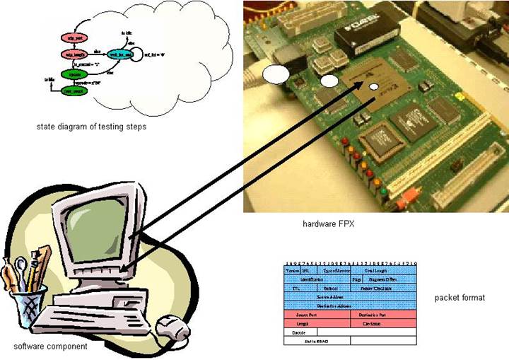
The testing part of this project includes software programs and the peripheral hardware circuits. Software RSA we use MyRSA java program written by Bobby Kenny(borrisoleigh@hotmail.com). Due to the length of the keys and n, we have to buffer inputs and outputs. However the buffering methods are different. For input a 1024-bit value can take up to 32 clock cycles to pass through under the assumption that each line in a packet is processed through one clock cycle. For output since the Opp module can take at most 256 bit input, so we also have a module ( not shown in the graph) that buffer the output value and send out 4 consecutive packets to Opp module.
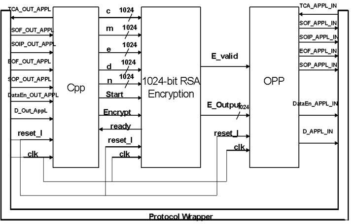
The Protocol Wrapper handles the header of the packets, reduces the workload of the modules inside. It does require some delay to finish processing the incoming packets and have limited bandwidth to send out packets.
In further detail, a state machine is implemented in the cpp module. Each clock cycle, a word is read into a 32-bit buffer. After all the values for encryption and\or decryption are gotten and after checking that the “ready” signal is OK from the RSA encryption module, it will then send out “start” signal to RSA encryption module, as well as the signals of the several 1024-bit values. The Opp module will generate packets whenever it detects ‘e_valid” signal. There are about seven input and output signals bordering between the internal modules and the outside packets. In the diagram, flip-flops haven’t been drawn at the borders for space purpose. The flip-flops guarantee the timing of the signals to arrive or leave the internal components. After the opp module creates the packets, we can then compare the value with the software calculation result.
An overall picture of the RSA hardware implementation on FPX
Уважаемый посетитель!
Чтобы распечатать файл, скачайте его (в формате Word).
Ссылка на скачивание - внизу страницы.